- 您現(xiàn)在的位置:買賣IC網(wǎng) > PDF目錄379475 > UC2907L (Texas Instruments, Inc.) I2C LCD VCOM calibrator PDF資料下載
參數(shù)資料
| 型號: | UC2907L |
| 廠商: | Texas Instruments, Inc. |
| 英文描述: | I2C LCD VCOM calibrator |
| 中文描述: | 負(fù)載共享規(guī)控制器 |
| 文件頁數(shù): | 1/7頁 |
| 文件大小: | 269K |
| 代理商: | UC2907L |
UC1907
UC2907
UC3907
DESCRIPTION
The UC3907 family of Load Share Controller ICs provides all the necessary
features to allow multiple independent power modules to be paralleled such
that each module supplies only its proportionate share to total load current.
This sharing is accomplished by controlling each module’s power stage
with a command generated from a voltage feedback amplifier whose refer-
ence can be independently adjusted in response to a common share bus
voltage. By monitoring the current from each module, the current share bus
circuitry determines which paralleled module would normally have the high-
est output current and, with the designation of this unit as the master, ad-
justs all the other modules to increase their output current to within 2.5% of
that of the master.
The current share bus signal interconnecting all the paralleled modules is a
low-impedance, noise-insensitive line which will not interfere with allowing
each module to act independently should the bus become open or shorted
to ground. The UC3907 controller will reside on the output side of each
power module and its overall function is to supply a voltage feedback loop.
The specific architecture of the power stage is unimportant. Either switch-
ing or linear designs may be utilized and the control signal may be either di-
rectly coupled or isolated though the use of an opto coupler or other
isolated medium.
Other features of the UC3907 include 1.25% accurate reference: a
low-loss,
fixed
gain
current
sense
high-impedance voltage sensing capability, and a status indicator to desig-
nate which module is performing as master.
amplifier,
a
fully
differential,
Load Share Controller
FEATURES
Fully Differential High Impedance
Voltage Sensing
Accurate Current Amplifier for Precise
Current Sharing
Opto Coupler Driving Capability
1.25% Trimmed Reference
Master Status Indication
4.5V TO 35V Operation
SLUS165 - MARCH 1999
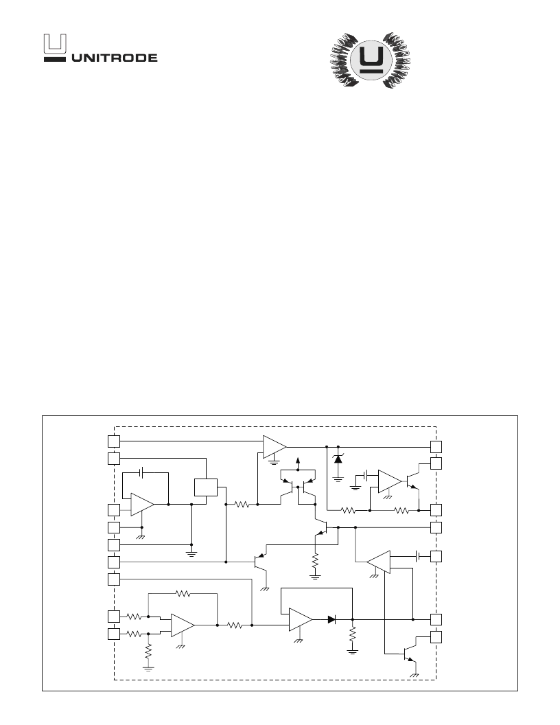
11
14
10
13
8
9
12
15
16
7
5
4
1
6
3
2
2k
2k
+
–
40k
40k
CURRENT SENSE
AMPLIFIER
100
+
–
BUFFER
AMPLIFIER
10k
+
–
+mV
ADJUST
AMPLIFIER
ADJ
17.5k
V
CC
1k
V
1.750V
+
–
GND
+
GROUND
AMPLIFIER
0.25V
DRV
50k
20k
+
1.0V
1.75V
VOLTAGE ERROR AMPLIFIER
STATUS INDICATE
CURRENT SHARE BUS
ADJ INPUT
ADJ OUT
ISET
OPTO DRIVE
COMP
(+) SENSE
VCC (4.5V TO 35V)
(–) SENSE
POWER RTN
ARTIFICIAL GND
VREF
C/S OUT
C/S (–)
C/S (+)
DRIVE
AMPLIFIER
+
–
BLOCK DIAGRAM
UDG-99052
相關(guān)PDF資料 |
PDF描述 |
|---|---|
| UC2907Q | Vertical Deflection Booster for 3-App TV/Monitor Applications with 70-V Flyback Generator |
| UC2907QTR | VERTICAL DEFLECTION BOOSTER FOR 2 APP MONITOR/TV APPLICATIONS WITH 70 V FLYBACK GENERATOR |
| UC3907QTR | Relay driver IC |
| UC3625J | Brushless DC Motor Controller |
| UC2625J | Brushless DC Motor Controller |
相關(guān)代理商/技術(shù)參數(shù) |
參數(shù)描述 |
|---|---|
| UC2907N | 功能描述:其他電源管理 LOAD SHARE CONTROLLER RoHS:否 制造商:Texas Instruments 輸出電壓范圍: 輸出電流:4 mA 輸入電壓范圍:3 V to 3.6 V 輸入電流: 功率耗散: 工作溫度范圍:- 40 C to + 110 C 安裝風(fēng)格:SMD/SMT 封裝 / 箱體:VQFN-48 封裝:Reel |
| UC2907NG4 | 功能描述:其他電源管理 LOAD SHARE CONTROLLER RoHS:否 制造商:Texas Instruments 輸出電壓范圍: 輸出電流:4 mA 輸入電壓范圍:3 V to 3.6 V 輸入電流: 功率耗散: 工作溫度范圍:- 40 C to + 110 C 安裝風(fēng)格:SMD/SMT 封裝 / 箱體:VQFN-48 封裝:Reel |
| UC2907Q | 制造商:TI 制造商全稱:Texas Instruments 功能描述:Load-Sharing Regulation Controller |
| UC2907QTR | 制造商:TI 制造商全稱:Texas Instruments 功能描述:Load-Sharing Regulation Controller |
| UC2908D | 制造商:Rochester Electronics LLC 功能描述: |
發(fā)布緊急采購,3分鐘左右您將得到回復(fù)。