- 您現(xiàn)在的位置:買賣IC網(wǎng) > PDF目錄378727 > UCC3952 (Texas Instruments, Inc.) Enhanced Single Cell Lithium-Ion Battery Protection IC PDF資料下載
參數(shù)資料
| 型號(hào): | UCC3952 |
| 廠商: | Texas Instruments, Inc. |
| 英文描述: | Enhanced Single Cell Lithium-Ion Battery Protection IC |
| 中文描述: | 增強(qiáng)的單節(jié)鋰離子電池保護(hù)IC |
| 文件頁(yè)數(shù): | 3/5頁(yè) |
| 文件大小: | 35K |
| 代理商: | UCC3952 |
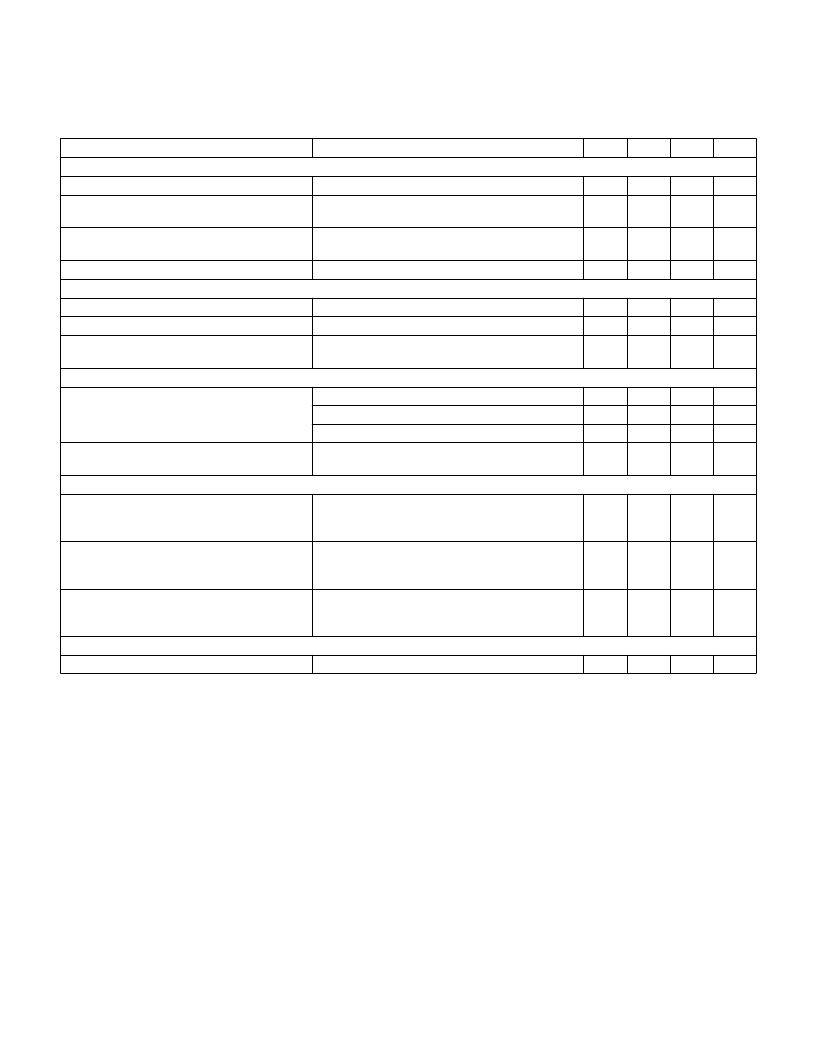
3
UCC3952-1/-2/-3/-4
ELECTRICAL CHARACTERISTICS:
Temperature Range: –20°C < T
A
< 70°C, Unless otherwise stated. All voltages are
with respect to BNEG. T
A
= T
J
PARAMETER
TEST CONDITIONS
State Transition Threshold Section (cont.)
OV Delay Time (T
OV
)
NORM to UV (V
UV
)
UCC3952-1, UCC3952-2, UCC3952-3,
UCC3952-4
UV to NORM (V
UVR)
UCC3952-1, UCC3952-2, UCC3952-3,
UCC3952-4
Overdischarge Delay Time (T
OD
)
Short Circuit Protection Section
ITHLD
Discharge current limit, PACK+ = 3.7V
TDLY
Discharge current delay, PACK+ = 3.7V, I = 6A
R
RESET
Discharge current reset resistance,
PACK+ = 4.0
Bias Section
IDD
Normal operating current. V
UV
< V
PACK
< V
OV
Operating current in overvoltage V
OV
< V
PACK
Shutdown operating current V
PACK
< V
UV
V
MIN
Minimum cell voltage when all circuits are
guaranteed to be fully functional
FET Switch Section
V
PACK
–
PACK+ > V
OV
, I(SWITCH) = 1mA to 2A
Battery overcharged state switch permits
discharge current only.
V
PACK
–
PACK+ = 2.5V, I(SWITCH) = –1mA to –2A
Battery overdischarged state switch permits
charge current only.
R
ON
In Normal Mode (when not in OV or UV). This
value includes package and bondwire resistance.
PACK+ = 2.5V
Thermal Shutdown Section
TS
Thermal shutdown temperature. (Note 1)
MIN
TYP
MAX
UNITS
1
2
sec
V
2.25
2.35
2.45
2.55
2.65
2.75
V
10
25
40
ms
3.0
1
7.5
4.5
2.5
A
ms
M
5
8
μ
A
μ
A
μ
A
V
11
24
2.5
1.7
100
400
mV
–600
–100
mV
50
75
m
135
°
C
Note 1. This parameter is guaranteed by design. Not 100% tested in production.
BNEG
: Connect the negative terminal of the battery to
this pin.
PACK+
: Connect to the positive terminal of the battery.
This pin is available to the user.
CBPS
: This power supply bypass pin is connected to
PACK+ through an internal 10K resistor.
0.1 F capacitor must be connected between this pin and
BNEG.
An external
PACK–
: The negative terminal of the battery pack (nega-
tive terminal available to the user).
switch connects this terminal to the BNEG terminal to
The internal FET
give the battery pack user appropriate access to the bat-
tery. In an over-charged state, only discharge current is
permitted. In an over-discharged state, only charge cur-
rent is permitted.
SUB
: (DP Package Only) Do not connect. These pins
must be electrically isolated from all other pins. These
pins may be soldered to isolated coppper pads for
heatsinking. However, most applications do not require
heatsinking.
TCLK
: Production Test Mode pin. This pin is used to
provide a high frequency clock to the IC during produc-
tion testing. In an application this pin may be left uncon-
nected, or tied to BNEG.
PIN DESCRIPTIONS
相關(guān)PDF資料 |
PDF描述 |
|---|---|
| UCC3952DP-3 | ER 19C 19#12 PIN PLUG |
| UCC3952DP-4 | Enhanced Single Cell Lithium-Ion Battery Protection IC |
| UCC3952PW-1 | SINGLE-CELL LITHIUM-LON BATTERY PROTECTION IC |
| UCC3952PW-2 | SINGLE-CELL LITHIUM-LON BATTERY PROTECTION IC |
| UCC3952PW-3 | SINGLE-CELL LITHIUM-LON BATTERY PROTECTION IC |
相關(guān)代理商/技術(shù)參數(shù) |
參數(shù)描述 |
|---|---|
| UCC3952AEVM-001 | 制造商:Rochester Electronics LLC 功能描述:- Bulk 制造商:Texas Instruments 功能描述: |
| UCC3952AEVM-002 | 制造商:Rochester Electronics LLC 功能描述:- Bulk |
| UCC3952AEVM-003 | 制造商:Rochester Electronics LLC 功能描述:- Bulk |
| UCC3952AEVM-004 | 制造商:Rochester Electronics LLC 功能描述:- Bulk 制造商:Texas Instruments 功能描述: |
| UCC3952AGSH-1 | 制造商:Rochester Electronics LLC 功能描述:- Bulk |
發(fā)布緊急采購(gòu),3分鐘左右您將得到回復(fù)。