- 您現(xiàn)在的位置:買賣IC網(wǎng) > PDF目錄361583 > UPC2251H Analog IC PDF資料下載
參數(shù)資料
| 型號: | UPC2251H |
| 英文描述: | Analog IC |
| 中文描述: | 模擬IC |
| 文件頁數(shù): | 2/12頁 |
| 文件大小: | 72K |
| 代理商: | UPC2251H |
Data Sheet G14451EJ2V0DS00
2
μ
PC2250 SERIES
ABSOLUTE MAXIMUM RATINGS (Unless otherwise specified, T
A
= 25°C)
Parameter
Symbol
Rating
Unit
Input Voltage
V
IN
–0.3 to +12
V
Total Power Dissipation
P
T
1.2
Note
W
Operating Ambient Temperature
T
A
–20 to +85
°
C
Operating Junction Temperature
T
J
–20 to +150
°
C
Storage Temperature
T
stg
–55 to +150
°
C
Thermal Resistance (Junction to Case)
R
th (J–C)
10
°
C/W
Thermal Resistance (Junction to Ambient)
R
th (J–A)
104
°
C/W
Note
The total loss is limited by an internal circuit. Where T
J
> 150°C, an internal protection circuit cuts off the
output.
Caution If any of the parameters exceeds the absolute maximum ratings, even momentarily, the quality of
the product may be impaired. The absolute maximum ratings are values that may physically
damage the product(s). Be sure to use the product(s) within the ratings.
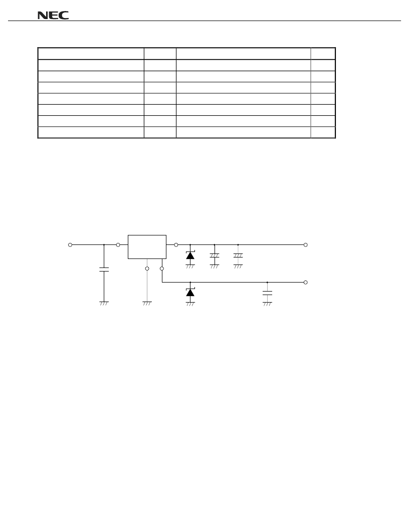
STANDARD CONNECTION
INPUT
INPUT
Output
Backup capacitor
(for backup)
Reset output
0.33
F
C
IN
μ
D
1
C
O
D
2
C
DLY
GND
RESET
OUTPUT
+
+
1
4
3
2
C
IN
: Determine the capacitance depending on the line between the power supply smoothing circuit and input pin.
Be sure to connect this capacitor to prevent abnormal oscillation. Use of a capacitor, such as a film
capacitor, with excellent voltage and temperature characteristics is recommended. Note that some
laminated ceramic capacitors have poor temperature and voltage characteristics. When using a laminated
ceramic capacitor, the capacitance must be stable in the voltage and temperature ranges used.
: Must be 10 μF or more. Be sure to connect this capacitor to prevent oscillation and to improve transient
load stability.
Connect C
IN
and C
O
as close to the IC (within 1 to 2 cm) as possible.
D
1
, D
2
: Connect Schottky barrier diodes (with a low forward voltage) if the voltage on the OUTPUT and RESET pins
is lower than that on the GND pin.
C
O
相關(guān)PDF資料 |
PDF描述 |
|---|---|
| UPC2253H | Analog IC |
| UPC2255H | Analog IC |
| UPC2260 | UPC2260 Data Sheet | Data Sheet[06/2000] |
| UPC2260V | Analog IC |
| UPC2800AHA | Remote-Control Amplifier/Preamplifier |
相關(guān)代理商/技術(shù)參數(shù) |
參數(shù)描述 |
|---|---|
| UPC2253H | 制造商:Renesas Electronics Corporation 功能描述: |
| UPC2255H | 制造商:未知廠家 制造商全稱:未知廠家 功能描述:Analog IC |
| UPC2260 | 制造商:NEC 制造商全稱:NEC 功能描述:LOW DROPOUT VOLTAGE REGULATOR WITH SYSTEM RESET PIN |
| UPC2260V | 制造商:NEC 制造商全稱:NEC 功能描述:LOW DROPOUT VOLTAGE REGULATOR WITH SYSTEM RESET PIN |
| UPC2300ACA | 制造商:Panasonic Industrial Company 功能描述:IC |
發(fā)布緊急采購,3分鐘左右您將得到回復(fù)。