- 您現(xiàn)在的位置:買賣IC網(wǎng) > PDF目錄379493 > UPD16661AN (NEC Corp.) 160-OUTPUT LCD COLUMN SEGMENT DRIVER WITH RAM PDF資料下載
參數(shù)資料
| 型號: | UPD16661AN |
| 廠商: | NEC Corp. |
| 英文描述: | 160-OUTPUT LCD COLUMN SEGMENT DRIVER WITH RAM |
| 中文描述: | 160輸出LCD列段驅動與RAM |
| 文件頁數(shù): | 2/36頁 |
| 文件大小: | 187K |
| 代理商: | UPD16661AN |
第1頁當前第2頁第3頁第4頁第5頁第6頁第7頁第8頁第9頁第10頁第11頁第12頁第13頁第14頁第15頁第16頁第17頁第18頁第19頁第20頁第21頁第22頁第23頁第24頁第25頁第26頁第27頁第28頁第29頁第30頁第31頁第32頁第33頁第34頁第35頁第36頁
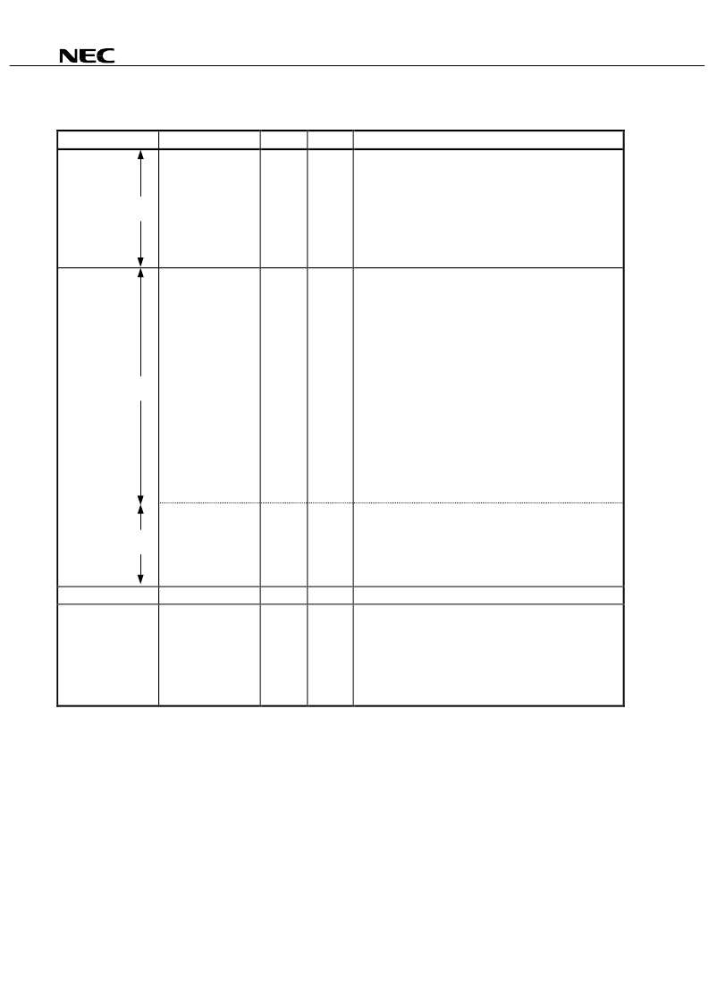
2
μ
PD16661A
PIN NAMES
Classification
Pin Name
Note
I/O
Pad No.
Function
CPU interface
D0 to D15
A0 to A16
/CS
/OE
/WE
/UBE
RDY
I/O
I
I
I
I
I
O
Data bus : 16 bits
Address bus : 17 bits
Chip select
Read signal
Write signal
Upper byte enable
Ready signal to CPU (Ready state at "H")
Control signals
PL0
PL1
PL2
DIR
MS
BMODE
GMODE
/REFRH
TEST
/RESET
/DOFF
OSC1
OSC2
STB
/FRM
L1
L2
/DOUT
I
I
I
I
I
I
I
I/O
I
I
I
I/O
I/O
I/O
I/O
O
Specifies the LSI placement positions (No. 0 to 7)
Specifies the LSI placement positions (No. 0 to 7)
Specifies the LSI placement positions (No. 0 to 7)
Specifies the liquid-crystal panel placement direction
Master/slave selection pin (Master mode at "H")
Data bus bit selection pin ("H" = 8 bits, "L" = 16 bits)
Gray scale data weight reverse switching
(When data = [1,1], "L" = black, "H" = white)
Self-diagnosis reset pin (wired-OR connection)
Test pin ("H" = test mode, on-chip pull-down resistor)
Reset signal
Display OFF input signal
Oscillator externally-attached resistor pin
Oscillator externally-attached resistor pin
Column drive signal (MS pin "H" = output, MS pin "L" = input)
Frame signal (MS pin "H" = output, MS pin "L" = input)
Row driver drive level selection signal (1st line)
Row driver drive level selection signal (2nd line)
Display OFF output signal
Liquid-crystal drive
Y1 to Y160
O
Liquid-crystal drive output
Power supplies
GND
V
CC1
V
CC2
V
0
V
1
V
2
Ground (two pins for V
CC1
system , three pins for V
CC2
system)
5-V power supply
3.3-V power supply
Liquid-crystal drive analog power supply
Liquid-crystal drive analog power supply
Liquid-crystal drive analog power supply
Note
3.3-V pin : D0 to D15, A0 to A16, /CS, /OE, /WE, /UBE, RDY, BMODE, GMODE, PL0, PL1, PL2, DIR, OSC1,
OSC2, /RESET, /DOFF, TEST, MS
5-V pin : STB, /FRM, L1, L2, /DOUT
Remark
/xxx indicates active low signal.
3.3 V
3.3 V
5.0 V
#
相關PDF資料 |
PDF描述 |
|---|---|
| UPD16661A | 160-OUTPUT LCD COLUMN SEGMENT DRIVER WITH RAM |
| UPD16675AN-051 | 1/34, 1/36 DUTY LCD CONTROLLER/DRIVER |
| UPD16675A | 1/34, 1/36 DUTY LCD CONTROLLER/DRIVER |
| UPD16675AN | 1/34, 1/36 DUTY LCD CONTROLLER/DRIVER |
| UPD16675AP | 1/34, 1/36 DUTY LCD CONTROLLER/DRIVER |
相關代理商/技術參數(shù) |
參數(shù)描述 |
|---|---|
| UPD16661AN-051 | 制造商:NEC 制造商全稱:NEC 功能描述:160-OUTPUT LCD COLUMN SEGMENT DRIVER WITH RAM |
| UPD16661AN-XXX | 制造商:未知廠家 制造商全稱:未知廠家 功能描述:LCD Display Driver |
| UPD16662 | 制造商:NEC 制造商全稱:NEC 功能描述:240 OUTPUT LCD COLUMN SEGMENT DRIVER WITH BUILT-IN RAM |
| UPD16662N | 制造商:NEC 制造商全稱:NEC 功能描述:240 OUTPUT LCD COLUMN SEGMENT DRIVER WITH BUILT-IN RAM |
| UPD16662N-051 | 制造商:NEC 制造商全稱:NEC 功能描述:240 OUTPUT LCD COLUMN SEGMENT DRIVER WITH BUILT-IN RAM |
發(fā)布緊急采購,3分鐘左右您將得到回復。