- 您現(xiàn)在的位置:買賣IC網(wǎng) > PDF目錄376428 > UPD6126A (NEC Corp.) 4-BIT SINGLE CHIP MICROCONTROLLER FOR REMOTE CONTROL TRANSMISSION PDF資料下載
參數(shù)資料
| 型號(hào): | UPD6126A |
| 廠商: | NEC Corp. |
| 英文描述: | 4-BIT SINGLE CHIP MICROCONTROLLER FOR REMOTE CONTROL TRANSMISSION |
| 中文描述: | 4位單片機(jī)的遙控傳輸 |
| 文件頁數(shù): | 8/40頁 |
| 文件大?。?/td> | 286K |
| 代理商: | UPD6126A |
第1頁第2頁第3頁第4頁第5頁第6頁第7頁當(dāng)前第8頁第9頁第10頁第11頁第12頁第13頁第14頁第15頁第16頁第17頁第18頁第19頁第20頁第21頁第22頁第23頁第24頁第25頁第26頁第27頁第28頁第29頁第30頁第31頁第32頁第33頁第34頁第35頁第36頁第37頁第38頁第39頁第40頁

μ
PD6125A, 6126A
8
10. TIMER
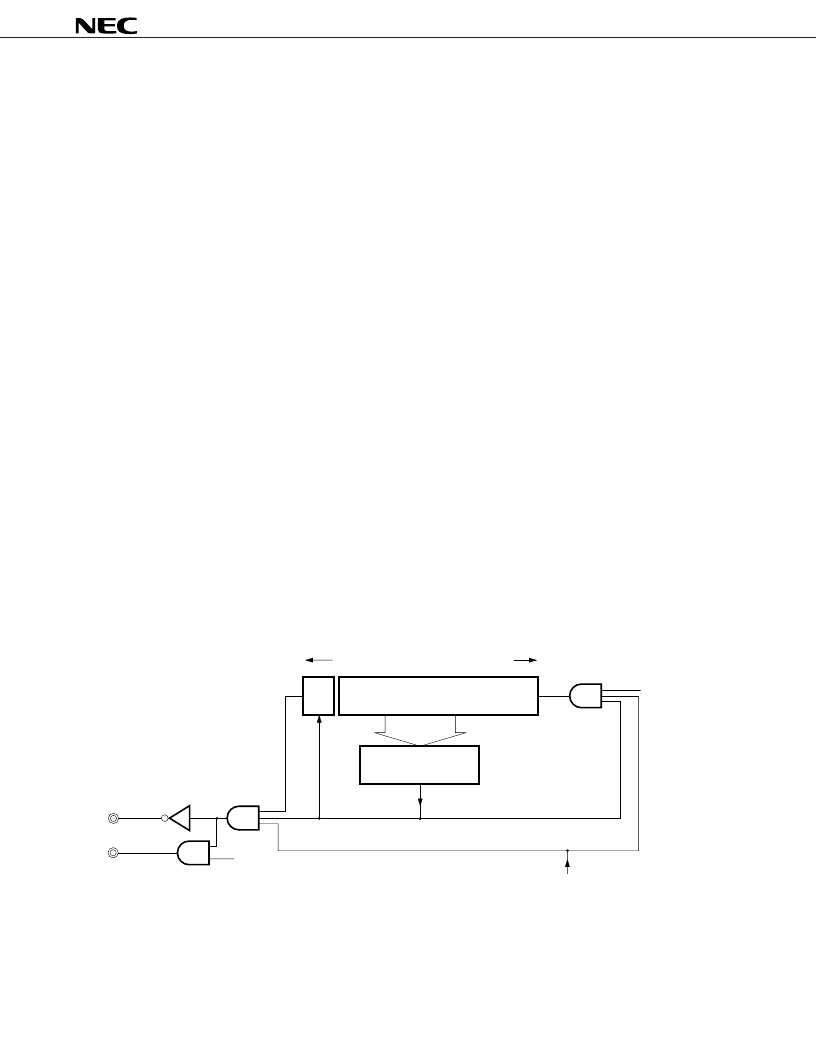
The timer block determines the transmission output pattern. The timer consists of 10 bits, of which 9 bits serve
as the 9-bit down counter and the remaining 1 bit serves as the 1-bit latch, which determines the carrier output validity.
The 9-bit down counter is decremented (-1) every 8/f
OSC
(s) in synchronization with the machine cycle, after starting
down count operation. Down counting stops after all of the 9 bits become 0. When down counting is stopped, the
signal indicating that the timer operation has stopped, is output. If the CPU is at standby (HALT TIMER) for the timer
operation completion, the standby (HALT) condition is released and the next instruction will be executed. If the next
instruction again sets the value of the down counter, down counting continues without any error (the carrier output
of the REM pin is not affected).
Set the down count time according to the following calculation; (set value (HEX) + 1) x 8/f
OSC
. Setting the value
to the timer is done by the timer manipulation instruction.
When the down counter is operating, the remote control transmission carrier can be output to the REM pin. Whether
or not to output the carrier can be selected by the MSB for the timer register block. Set “1”, when outputting the carrier,
or “0”, when not outputting the carrier.
If all the down counter bits become “0”, when outputting the carrier, the carrier output will be stopped. When not
outputting the carrier, the REM pin output will become low level.
A signal in synchronization with the REM output is output to the S-OUT pin. However, the waveform for the S-
OUT pin is low, when the carrier is being output to the REM pin, or it is high, when the carrier is not being output to
the REM pin.
If the HALT instruction, which initiates the oscillation stop mode, is executed when the down counter is operating,
the oscillation stop mode is initiated after down counting is stopped (after 0).
Timer operation STOP/RUN is controlled by the control register (P
1
). (Refer to 13. CONTROL REGISTER (P
1
).)
When “all clear” is input or on reset, the REM pin goes low and S-OUT pin goes high. All 10 bits of the timer are
cleared to 000H.
Caution
Because the timer clock is not synchronized with the carrier output, the pulse width may be
shortened at the beginning and end of the carrier output.
Figure 10-1. Timer Block Organization
S–OUT
REM
Carrier
(fosc/12, fosc/8)
Selected by control register
Clear
Set by timer mainpulation instruction
9-bit down counter
Zero detection circuit
D of control register P
(Timer RUN/STOP)
1
1/0
MSB
fosc / 8
相關(guān)PDF資料 |
PDF描述 |
|---|---|
| UPD6126AG | 4-BIT SINGLE CHIP MICROCONTROLLER FOR REMOTE CONTROL TRANSMISSION |
| UPD6125A | 4-BIT SINGLE CHIP MICROCONTROLLER FOR REMOTE CONTROL TRANSMISSION |
| UPD6125AG | 4-BIT SINGLE CHIP MICROCONTROLLER FOR REMOTE CONTROL TRANSMISSION |
| UPD65664 | CMOS-6/6A/6V/6X 1.0-MICRON CMOS GATE ARRAYS |
| UPD65672 | CMOS-6/6A/6V/6X 1.0-MICRON CMOS GATE ARRAYS |
相關(guān)代理商/技術(shù)參數(shù) |
參數(shù)描述 |
|---|---|
| UPD6126AG | 制造商:NEC 制造商全稱:NEC 功能描述:4-BIT SINGLE CHIP MICROCONTROLLER FOR REMOTE CONTROL TRANSMISSION |
| UPD6127CS | 制造商:未知廠家 制造商全稱:未知廠家 功能描述:Remote-Control Transmitter/Encoder |
| UPD6127GS | 制造商:未知廠家 制造商全稱:未知廠家 功能描述:Remote-Control Transmitter/Encoder |
| UPD6129CS | 制造商:未知廠家 制造商全稱:未知廠家 功能描述:Remote-Control Transmitter/Encoder |
| UPD6129GS | 制造商:未知廠家 制造商全稱:未知廠家 功能描述:Remote-Control Transmitter/Encoder |
發(fā)布緊急采購(gòu),3分鐘左右您將得到回復(fù)。