- 您現(xiàn)在的位置:買賣IC網(wǎng) > PDF目錄379501 > UPD72012CU (NEC Corp.) HUB CONTROLLER FOR UNIVERSAL SERIAL BUS PDF資料下載
參數(shù)資料
| 型號(hào): | UPD72012CU |
| 廠商: | NEC Corp. |
| 英文描述: | HUB CONTROLLER FOR UNIVERSAL SERIAL BUS |
| 中文描述: | 集線器控制器通用串行總線 |
| 文件頁(yè)數(shù): | 8/36頁(yè) |
| 文件大小: | 414K |
| 代理商: | UPD72012CU |
第1頁(yè)第2頁(yè)第3頁(yè)第4頁(yè)第5頁(yè)第6頁(yè)第7頁(yè)當(dāng)前第8頁(yè)第9頁(yè)第10頁(yè)第11頁(yè)第12頁(yè)第13頁(yè)第14頁(yè)第15頁(yè)第16頁(yè)第17頁(yè)第18頁(yè)第19頁(yè)第20頁(yè)第21頁(yè)第22頁(yè)第23頁(yè)第24頁(yè)第25頁(yè)第26頁(yè)第27頁(yè)第28頁(yè)第29頁(yè)第30頁(yè)第31頁(yè)第32頁(yè)第33頁(yè)第34頁(yè)第35頁(yè)第36頁(yè)
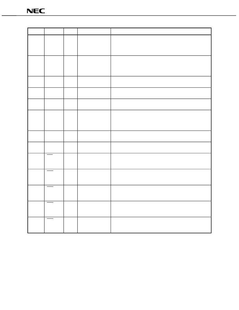
8
Data Sheet S13918EJ3V0DS
μ
PD72012
(2/3)
Pin No.
Note 1
Pin Name
I/O
Signal Name
Function
18(24)
AV
DD1
-
AVDD1
Power supply pin of on-chip clock drive circuit.
To stabilize the power supply, connect directly to a stable power
supply using the shortest wire possible or connect to GND via a
capacitor along the wire (3.3 V input).
19(25)
CLK / X2
I
CLOCK / XTAL
When you input a clock signal from an oscillator, input at the 48 MHz
CMOS level (5 V can be input).
When using a 4 MHz crystal oscillator, connect the oscillator to this
pin.
20(26)
X1
I
XTAL
When using a 4 MHz crystal oscillator, connect the oscillator to this
pin.
21(27)
AGND1
-
AGND1
GND pin of on-chip clock drive circuit.
Connect to GND.
22(28)
AGND2
-
AGND2
GND pin of on-chip frequency multiplier (PLL).
Connect to GND.
23(29)
AV
DD2
-
AVDD2
Power supply pin of on-chip frequency multiplier (PLL).
To stabilize the power supply, connect directly to a stable power
supply using the shortest wire possible or connect to GND via a
capacitor along the wire (3.3 V input).
24(30)
DV
DD
-
DVDD
(TS1)
Test pin of
μ
PD72012 (corresponds to TS1 pin in
μ
PD72011).
Connect to 3.3 V power supply.
25(31)
DGND
(Buffer)
-
DGND
(Buffer)
Connect to GND.
26(32)
CS1
I
PORTCURRENT1
Low active input pin that inputs overcurrent states detected by
external circuit of downstream port #1.
When not using this pin, connect it directly to V
DD
.
Note 2
27(33)
CS2
I
PORTCURRENT2
Low active input pin that inputs overcurrent states detected by
external circuit of downstream port #2.
When not using this pin, connect it directly to V
DD
.
Note 2
28(34)
CS3
I
PORTCURRENT3
Low active input pin that inputs overcurrent states detected by
external circuit of downstream port #3.
When not using this pin, connect it directly to V
DD
.
Note 2
29(35)
CS4
I
PORTCURRENT4
Low active input pin that inputs overcurrent states detected by
external circuit of downstream port #4.
When not using this pin, connect it directly to V
DD
.
Note 2
30(36)
CS5
I
PORTCURRENT5
Low active input pin that inputs overcurrent states detected by
external circuit of downstream port #5.
When not using this pin, connect it directly to V
DD
.
Note 2
Notes 1.
Pin numbers for QFP are shown in ( ).
For details, refer to
Table 1-3
in
1.2 Tables by Pin Function
.
2.
相關(guān)PDF資料 |
PDF描述 |
|---|---|
| UPD72012GB | HUB CONTROLLER FOR UNIVERSAL SERIAL BUS |
| UPD72012CU-XXX | HUB CONTROLLER FOR UNIVERSAL SERIAL BUS |
| UPD72012GB-XXX | HUB CONTROLLER FOR UNIVERSAL SERIAL BUS |
| UPD72012GB-XXX-3B4 | HUB CONTROLLER FOR UNIVERSAL SERIAL BUS |
| UPD72012 | HUB CONTROLLER FOR UNIVERSAL SERIAL BUS |
相關(guān)代理商/技術(shù)參數(shù) |
參數(shù)描述 |
|---|---|
| UPD720130GC-9EU-A | 制造商:NEC Electronics Corporation 功能描述:BRIDGE USB TO IDE SMD TQFP100 |
| UPD720133GB-YEU-A | 制造商:NEC Electronics Corporation 功能描述:IC BRIDGE USB TO IDE SMD TQFP64 |
| UPD720150F1-BAE-A | 制造商:Renesas Electronics Corporation 功能描述:USB2.0 HOST/DEVICE CTRL, 884-P |
| UPD720150GK-9EU-A | 制造商:Renesas Electronics Corporation 功能描述:USB2.0 HOST/DEVICE CTRL, 80-PI 制造商:Renesas Electronics Corporation 功能描述:USB2.0 HOST PERIPHERAL CONTROLLER - Bulk 制造商:Renesas Electronics Corporation 功能描述:RENUPD720150GK-9EU-A USB2.0 HOST IC |
| UPD720200A | 制造商:Renesas Electronics Corporation 功能描述: |
發(fā)布緊急采購(gòu),3分鐘左右您將得到回復(fù)。