- 您現(xiàn)在的位置:買賣IC網(wǎng) > PDF目錄378746 > UPD72870GM-8ED (NEC Corp.) IEEE1394 1-CHIP OHCI HOST CONTROLLER PDF資料下載
參數(shù)資料
| 型號(hào): | UPD72870GM-8ED |
| 廠商: | NEC Corp. |
| 英文描述: | IEEE1394 1-CHIP OHCI HOST CONTROLLER |
| 中文描述: | IEEE1394連接1 - OHCI主機(jī)控制器芯片 |
| 文件頁數(shù): | 26/48頁 |
| 文件大小: | 337K |
| 代理商: | UPD72870GM-8ED |
第1頁第2頁第3頁第4頁第5頁第6頁第7頁第8頁第9頁第10頁第11頁第12頁第13頁第14頁第15頁第16頁第17頁第18頁第19頁第20頁第21頁第22頁第23頁第24頁第25頁當(dāng)前第26頁第27頁第28頁第29頁第30頁第31頁第32頁第33頁第34頁第35頁第36頁第37頁第38頁第39頁第40頁第41頁第42頁第43頁第44頁第45頁第46頁第47頁第48頁
Preliminary Data Sheet S13925EJ2V0DS00
26
μ
PD72870,72871
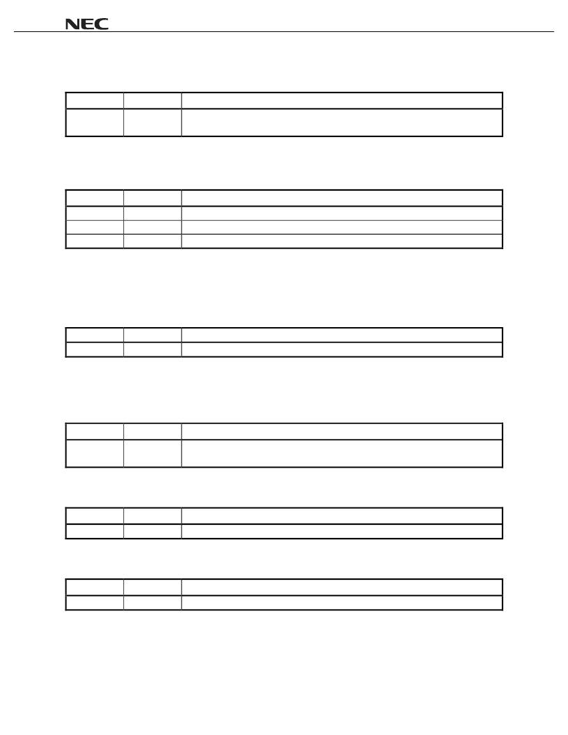
3.1.5 Offset_08 Revision ID Register
This register specifies a revision number assigned by NEC Corporation for the
μ
PD72870, 72871.
Bits
R/W
Description
7-0
R
Default value of 01H. It specifies the silicon revision. It will be incremented for subsequent
silicon revisions.
3.1.6 Offset_09 Class Code Register
This register identifies the class code, sub-class code, and programming interface of the
μ
PD72870, 72871.
Bits
R/W
Description
7-0
R
Constant value of 10H.
It specifies an IEEE1394 OpenHCI-compliant Host Controller.
15-8
R
Constant value of 00H. It specifies an “IEEE1394” type.
23-16
R
Constant value of 0CH. It specifies a “Serial Bus Controller”.
3.1.7 Offset_0C Cache Line Size Register
This register specifies the system cache line size, which is PC-host system dependent, in units of 32-bit words.
The following cache line sizes are supported: 2, 4, 8, 16, 32, 64, and 128. All other values will be recognized as 0,
i.e. cache disabled.
Bits
R/W
Description
7-0
R/W
Default value of 00H.
3.1.8 Offset_0D Latency Timer Register
This register defines the maximum amount of time that the
μ
PD72870, 72871 is permitted to retain ownership of
the bus after it has acquired bus ownership and initiated a subsequent transaction.
Bits
R/W
Description
7-0
R/W
Default value of 00H. It specifies the number of PCI-bus clocks that the
μ
PD72870, 72871 may
hold the PCI bus as a bus-master.
3.1.9 Offset_0E Header Type Register
Bits
R/W
Description
7-0
R
Constant value of 00H.
It specifies a single function device.
3.1.10 Offset_0F BIST Register
Bits
R/W
Description
7-0
R
Constant value of 00H.
It specifies whether the device is capable of Built-in Self Test.
相關(guān)PDF資料 |
PDF描述 |
|---|---|
| UPD750104GB-XXX-3BS-MTX | MICROCONTROLLER|4-BIT|UPD75XL CPU|CMOS|QFP|44PIN|PLASTIC |
| UPD750108CUA | 4 BIT SINGLE-CHIP MICROCONTROLLER |
| UPD750104 | 4 BIT SINGLE-CHIP MICROCONTROLLER |
| UPD750104A | 4 BIT SINGLE-CHIP MICROCONTROLLER |
| UPD750104CU | 4 BIT SINGLE-CHIP MICROCONTROLLER |
相關(guān)代理商/技術(shù)參數(shù) |
參數(shù)描述 |
|---|---|
| UPD74HC04C | 制造商:Panasonic Industrial Company 功能描述:IC |
| UPD750068GT-396 | 制造商:Renesas Electronics Corporation 功能描述: |
| UPD7507C189 | 制造商:Panasonic Industrial Company 功能描述:IC |
| UPD7508CU265 | 制造商:Panasonic Industrial Company 功能描述:IC |
| UPD75208 | 制造商:Panasonic Industrial Company 功能描述:IC |
發(fā)布緊急采購,3分鐘左右您將得到回復(fù)。