- 您現(xiàn)在的位置:買賣IC網(wǎng) > PDF目錄383983 > UPD75212A (NEC Corp.) 4-BIT SINGLE-CHIP MICROCOMPUTER PDF資料下載
參數(shù)資料
| 型號: | UPD75212A |
| 廠商: | NEC Corp. |
| 英文描述: | 4-BIT SINGLE-CHIP MICROCOMPUTER |
| 中文描述: | 4位單片機 |
| 文件頁數(shù): | 46/70頁 |
| 文件大小: | 516K |
| 代理商: | UPD75212A |
第1頁第2頁第3頁第4頁第5頁第6頁第7頁第8頁第9頁第10頁第11頁第12頁第13頁第14頁第15頁第16頁第17頁第18頁第19頁第20頁第21頁第22頁第23頁第24頁第25頁第26頁第27頁第28頁第29頁第30頁第31頁第32頁第33頁第34頁第35頁第36頁第37頁第38頁第39頁第40頁第41頁第42頁第43頁第44頁第45頁當前第46頁第47頁第48頁第49頁第50頁第51頁第52頁第53頁第54頁第55頁第56頁第57頁第58頁第59頁第60頁第61頁第62頁第63頁第64頁第65頁第66頁第67頁第68頁第69頁第70頁
46
μ
PD75212A
V
DD
V
LOAD
V
PRE
V
I
V
O
V
OD
I
OH
I
OL
P
T
T
opt
T
stg
UNIT
RATING
TEST CONDITIONS
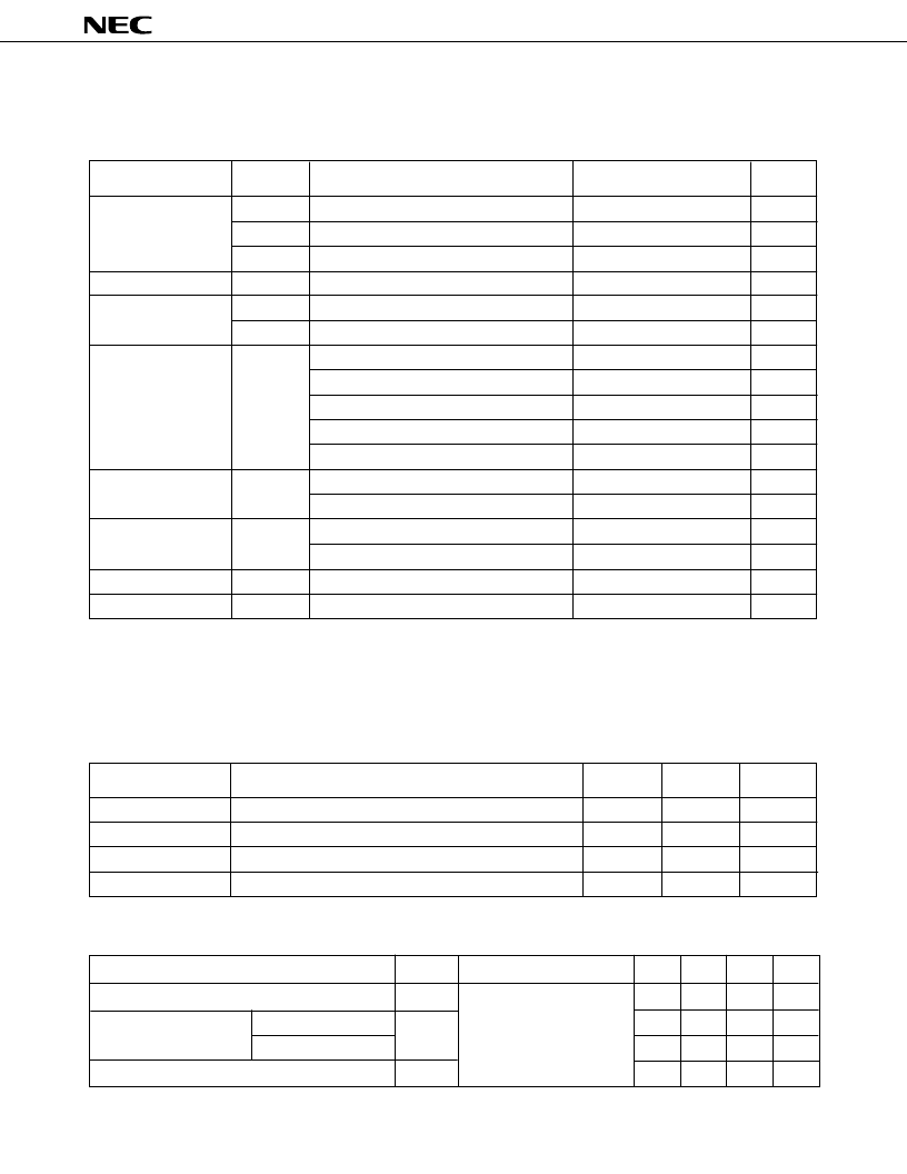
12. ELECTRICAL SPECIFICATIONS
ABSOLUTE MAXIMUM RATINGS (Ta = 25
°
C)
Power supply voltage
Input voltage
Output voltage
Output current high
Output current low
Total loss
*1
Operating temperature
Storage temperature
Pins except display output pins
Display output pins
1 pin except display output pins
S0 to S9
1 pin
T0 to T15
1 pin
Total of pins except display output pins
Total of display output pins
1 pin
Total of pins
Plastic QFP
Plastic shrink DIP
–0.3 to +7.0
V
DD
–40 to V
DD
+0.3
V
DD
–12 to V
DD
+0.3
–0.3 to V
DD
+0.3
–0.3 to V
DD
+0.3
V
DD
–40 to V
DD
+0.3
–15
–15
–30
–20
–120
17
60
450
600
–40 to +85
–65 to +150
V
V
V
V
V
V
mA
mA
mA
mA
mA
mA
mA
mW
mW
°
C
°
C
SYMBOL
PARAMETER
Note
Product quality may suffer if the absolute maximum rating is exceeded for even a single parameter, or even
momentarily. In other words, the absolute maximum ratings are rated values at which the product is on
the verge of suffering physical damage, and therefore, the product must be used under conditions which
ensure that the absolute maximum ratings are not exceeded.
OPERATING VOLTAGE (Ta = –40 to +85
°
C)
PARAMETER
CPU
*2
Display controller
Time/pulse generator
Other hardware
*2
TEST CONDITIONS
MIN.
*3
4.5
4.5
2.7
MAX.
UNIT
6.0
6.0
6.0
6.0
V
V
V
V
Input capacitance
Except display output
Display output
Input /output capacitance
UNIT
Output capacitance
PARAMETER
SYMBOL
C
IN
C
IO
pF
pF
pF
pF
MAX.
15
15
35
15
TYP.
MIN.
TEST CONDITIONS
f = 1 MHz
Unmeasured pin returned
to 0 V
C
OUT
CAPACITANCE ( Ta = 25
°
C, V
DD
= 0 V )
#
相關PDF資料 |
PDF描述 |
|---|---|
| UPD75212ACW | 4-BIT SINGLE-CHIP MICROCOMPUTER |
| UPD75212AGF | 4-BIT SINGLE-CHIP MICROCOMPUTER |
| UPD75216 | 4-BIT SINGLE-CHIP MICROCOMPUTER |
| UPD75216A | 4-BIT SINGLE-CHIP MICROCOMPUTER |
| UPD75216ACW | 4-BIT SINGLE-CHIP MICROCOMPUTER |
相關代理商/技術參數(shù) |
參數(shù)描述 |
|---|---|
| UPD753012AGC-P33-8BT-A | 制造商:Renesas Electronics Corporation 功能描述: |
| UPD753016AGC-P29-8BT | 制造商:Renesas Electronics Corporation 功能描述: |
| UPD75304GF-407-3B9 | 制造商:Renesas Electronics Corporation 功能描述: |
| UPD75306G182 | 制造商:Panasonic Industrial Company 功能描述:IC |
| UPD75308F478 | 制造商:Panasonic Industrial Company 功能描述:IC |
發(fā)布緊急采購,3分鐘左右您將得到回復。