- 您現(xiàn)在的位置:買賣IC網(wǎng) > PDF目錄379503 > UPD75304BGC (NEC Corp.) 4-BIT SINGLE-CHIP MICROCOMPUTER PDF資料下載
參數(shù)資料
| 型號: | UPD75304BGC |
| 廠商: | NEC Corp. |
| 英文描述: | 4-BIT SINGLE-CHIP MICROCOMPUTER |
| 中文描述: | 4位單片機(jī) |
| 文件頁數(shù): | 16/76頁 |
| 文件大?。?/td> | 572K |
| 代理商: | UPD75304BGC |
第1頁第2頁第3頁第4頁第5頁第6頁第7頁第8頁第9頁第10頁第11頁第12頁第13頁第14頁第15頁當(dāng)前第16頁第17頁第18頁第19頁第20頁第21頁第22頁第23頁第24頁第25頁第26頁第27頁第28頁第29頁第30頁第31頁第32頁第33頁第34頁第35頁第36頁第37頁第38頁第39頁第40頁第41頁第42頁第43頁第44頁第45頁第46頁第47頁第48頁第49頁第50頁第51頁第52頁第53頁第54頁第55頁第56頁第57頁第58頁第59頁第60頁第61頁第62頁第63頁第64頁第65頁第66頁第67頁第68頁第69頁第70頁第71頁第72頁第73頁第74頁第75頁第76頁
16
μ
PD75304B,75306B,75308B
3.5
PRECAUTIONS CONCERNING P00/INT4 PIN AND RESET PIN
In addition to the functions shown in 3.1 and 3.2, the P00/INT4 pin and RESET pin are also used to set the
test mode for testing internal
μ
PD75308B operation (for IC testing).
The test mode is set when a voltage greater than V
DD
is applied to either of these pins. Consequently, if
noise exceeding V
DD
is applied during normal operation, the test mode may be entered, making it impossible
for normal operation to continue.
For example, misoperation may result if inter-wiring noise is applied to the P00/INT4 or RESET pin due to
the length of the wiring from these pins, and the pin voltage exceeds V
DD
.
Wiring should therefore be carried out so that inter-wiring noise is suppressed as far as possible. If it is
completely impossible to suppress noise, noise prevention measures should be taken using an external compo-
nent as shown below.
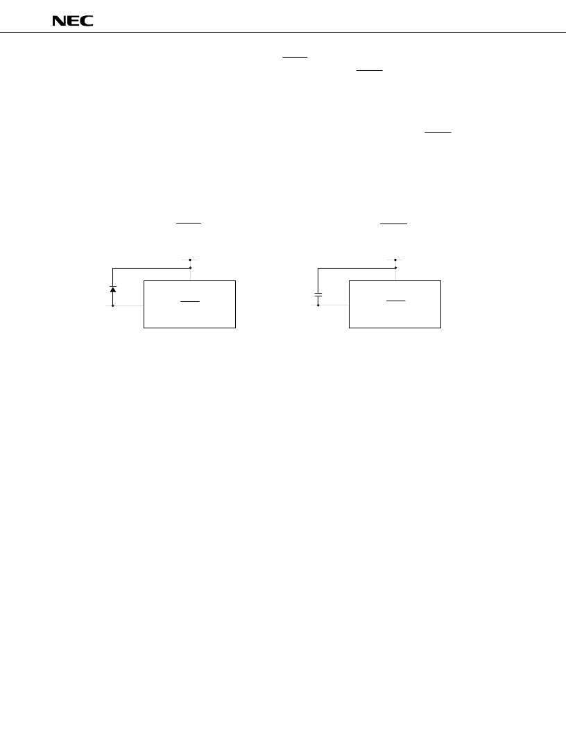
o
Diode connected between
P00/INT4 or RESET and V
DD
o
Capacitor connected between
P00/INT4 or RESET and V
DD
Diode with
Small V
F
V
DD
V
DD
V
DD
P00/INT4, RESET
V
DD
P00/INT4, RESET
4. MEMORY CONFIGURATION
Program memory (ROM) ... 8064
×
8 bits (0000H to 1F7FH):
μ
PD75308B
6016
×
8 bits (0000H to 177FH):
μ
PD75306B
4096
×
8 bits (0000H to 0FFFH):
μ
PD75304B
0000H to 0001H: Vector table in which the program start address after a reset is written.
0002H to 000BH: Vector table in which program start addresses in case of interrupts are written.
0020H to 007FH: Table area referenced by the GETI instruction.
Data memory
Data area ... 512
×
4 bits (000H to 1FFH)
Peripheral hardware area ... 128
×
4 bits (F80H to FFFH)
#
相關(guān)PDF資料 |
PDF描述 |
|---|---|
| UPD75304BGF | 4-BIT SINGLE-CHIP MICROCOMPUTER |
| UPD75304BGK | 4-BIT SINGLE-CHIP MICROCOMPUTER |
| UPD75306B | 4-BIT SINGLE-CHIP MICROCOMPUTER |
| UPD75306BGC | 4-BIT SINGLE-CHIP MICROCOMPUTER |
| UPD75306BGF | 4-BIT SINGLE-CHIP MICROCOMPUTER |
相關(guān)代理商/技術(shù)參數(shù) |
參數(shù)描述 |
|---|---|
| UPD75304GF-407-3B9 | 制造商:Renesas Electronics Corporation 功能描述: |
| UPD75306G182 | 制造商:Panasonic Industrial Company 功能描述:IC |
| UPD75308F478 | 制造商:Panasonic Industrial Company 功能描述:IC |
| UPD75308G699 | 制造商:Panasonic Industrial Company 功能描述:IC |
| UPD753204013 | 制造商:Panasonic Industrial Company 功能描述:IC |
發(fā)布緊急采購,3分鐘左右您將得到回復(fù)。