- 您現(xiàn)在的位置:買賣IC網(wǎng) > PDF目錄384045 > UPD75402A (NEC Corp.) 4 BIT SINGLE-CHIP MICROCOMPUTER PDF資料下載
參數(shù)資料
| 型號(hào): | UPD75402A |
| 廠商: | NEC Corp. |
| 英文描述: | 4 BIT SINGLE-CHIP MICROCOMPUTER |
| 中文描述: | 4位單片機(jī) |
| 文件頁數(shù): | 30/48頁 |
| 文件大小: | 515K |
| 代理商: | UPD75402A |
第1頁第2頁第3頁第4頁第5頁第6頁第7頁第8頁第9頁第10頁第11頁第12頁第13頁第14頁第15頁第16頁第17頁第18頁第19頁第20頁第21頁第22頁第23頁第24頁第25頁第26頁第27頁第28頁第29頁當(dāng)前第30頁第31頁第32頁第33頁第34頁第35頁第36頁第37頁第38頁第39頁第40頁第41頁第42頁第43頁第44頁第45頁第46頁第47頁第48頁
30
μ
PD75402A(A)
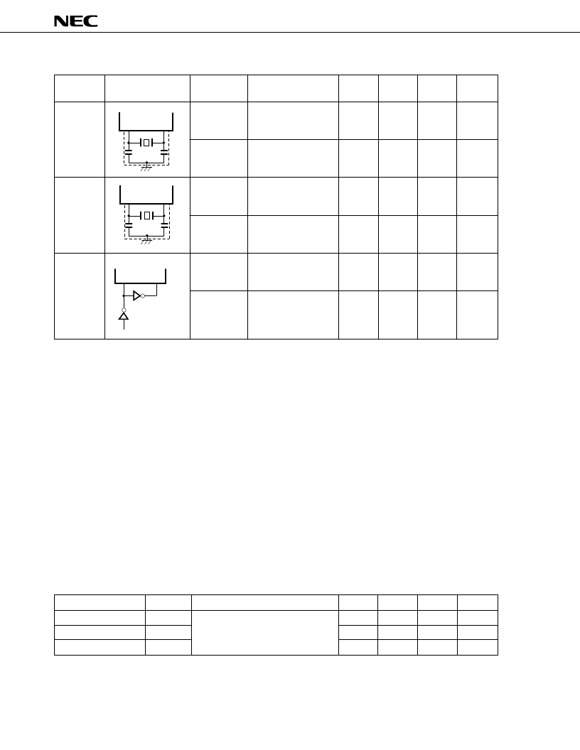
Resonator
Ceramic
resonator
Crystal
External
clock
Recommended
constant
Parameter
Oscillator
frequency
(f
XX
)
Note 1
Oscillation
settling time
Note 2
Oscillator
frequency
(f
XX
)
Note 1
Oscillation
settling time
Note 2
X1 input
frequency
(f
X
)
Note 1
X1 input
high/low
level width
(t
XH
, t
XL
)
CHARACTERISTICS OF THE OSCILLATION CIRCUIT
(T
a
= –40 to +85 C, V
DD
= 2.7 to 6.0 V)
Notes 1.
The oscillator frequency and X1 input frequency indicate only the oscillator characteristics. See
the item of AC characteristics for the instruction execution time.
2.
The oscillation settling time means the time required for the oscillation to settle after V
DD
is applied
or after the STOP mode is released.
3.
When 4.19 MHz < f
X
≤
5.0 MHz, do not select PCC = 0011 as the instruction execution time. When
PCC = 0011, one machine cycle falls short of 0.95
μ
s, the minimum value for the standard.
Caution When the clock oscillator is used, conform to the following guidelines when wiring at the
portions surrounded by dotted lines in the figures above to eliminate the influence of the wiring
capacity.
The wiring must be as short as possible.
Other signal lines must not run in these areas.
Any line carrying a high fluctuating current must be kept away as far as possible.
The grounding point of the capacitor of the oscillator must have the same potential as that
of V
SS
. It must not be grounded to ground patterns carrying a large current.
No signal must be taken from the oscillator.
CAPACITANCE
(T
a
= 25 C, V
DD
= 0 V)
Unit
MHz
ms
MHz
ms
MHz
ns
Min.
2.0
2.0
2.0
100
Typ.
4.19
Max.
5.0
Note 3
4
5.0
Note 3
10
5.0
Note 3
250
Conditions
V
DD
= oscillation
voltage range
After V
DD
reaches
MIN. of the oscilla-
tion voltage range
V
DD
= 4.5 to 6.0 V
X1
X2
C1
C2
X1
X2
C1
C2
X1
X2
μ
PD74HCU04
Parameter
Input capacitance
Output capacitance
I/O capacitance
Symbol
C
IN
C
OUT
C
IO
Min.
Typ.
Max.
15
15
15
Unit
pF
pF
pF
Conditions
f = 1 MHz
0 V for pins other than pins to be
measured
#
相關(guān)PDF資料 |
PDF描述 |
|---|---|
| UPD75402AA | 4 BIT SINGLE-CHIP MICROCOMPUTER |
| UPD75402AC | 4 BIT SINGLE-CHIP MICROCOMPUTER |
| UPD75402ACA | 4 BIT SINGLE-CHIP MICROCOMPUTER |
| UPD75402ACT | 4 BIT SINGLE-CHIP MICROCOMPUTER |
| UPD75402ACTA | 4 BIT SINGLE-CHIP MICROCOMPUTER |
相關(guān)代理商/技術(shù)參數(shù) |
參數(shù)描述 |
|---|---|
| UPD7554AG-597-E2 | 制造商:Renesas Electronics Corporation 功能描述: |
| UPD7554AG-597-E2-A | 制造商:Renesas Electronics Corporation 功能描述: |
| UPD7554AG-603-E2 | 制造商:Renesas Electronics Corporation 功能描述: |
| UPD7554AG-603-E2-A | 制造商:Renesas Electronics Corporation 功能描述: |
| UPD7554AG-611-E2 | 制造商:Renesas Electronics Corporation 功能描述: |
發(fā)布緊急采購,3分鐘左右您將得到回復(fù)。