- 您現(xiàn)在的位置:買賣IC網(wǎng) > PDF目錄379503 > UPD77210F1-DA2 (NEC Corp.) 16-BIT FIXED-POINT DIGITAL SIGNAL PROCESSOR PDF資料下載
參數(shù)資料
| 型號: | UPD77210F1-DA2 |
| 廠商: | NEC Corp. |
| 元件分類: | 數(shù)字信號處理 |
| 英文描述: | 16-BIT FIXED-POINT DIGITAL SIGNAL PROCESSOR |
| 中文描述: | 16位定點(diǎn)數(shù)字信號處理器 |
| 文件頁數(shù): | 28/74頁 |
| 文件大小: | 467K |
| 代理商: | UPD77210F1-DA2 |
第1頁第2頁第3頁第4頁第5頁第6頁第7頁第8頁第9頁第10頁第11頁第12頁第13頁第14頁第15頁第16頁第17頁第18頁第19頁第20頁第21頁第22頁第23頁第24頁第25頁第26頁第27頁當(dāng)前第28頁第29頁第30頁第31頁第32頁第33頁第34頁第35頁第36頁第37頁第38頁第39頁第40頁第41頁第42頁第43頁第44頁第45頁第46頁第47頁第48頁第49頁第50頁第51頁第52頁第53頁第54頁第55頁第56頁第57頁第58頁第59頁第60頁第61頁第62頁第63頁第64頁第65頁第66頁第67頁第68頁第69頁第70頁第71頁第72頁第73頁第74頁
Data Sheet U15203EJ3V0DS
28
μ
PD77210, 77213
4. RESET FUNCTION
The device is initialized when a low level of the specified width is input to the RESET pin.
4.1 Hardware Reset
The internal circuitry of the
μ
PD77210 Family is initialized when the RESET pin is asserted active (low level) for a
specific period. When the RESET pin is then deasserted inactive (high level), booting of the instruction RAM is
performed in accordance with the status of the port pins (P0, P1, P2, and P3), and then processing is executed
starting from the instruction at address 0x200 (reset entry) of the instruction memory.
5. FUNCTION OF BOOT-UP ROM
The instruction RAM is booted up by using the internal boot-up ROM when power is applied or when the contents
of the instruction memory are to be rewritten by the program.
5.1 Boot at Reset
Immediately after release of a hardware reset, the boot program first reads general-purpose I/O port pins P0 to
P3, and a boot mode (memory boot/host boot/serial boot) is determined by the bit patterns of these port pins. Once
the booting processing has been completed, processing is executed starting from the instruction at address 0x200
(reset entry) of the instruction memory.
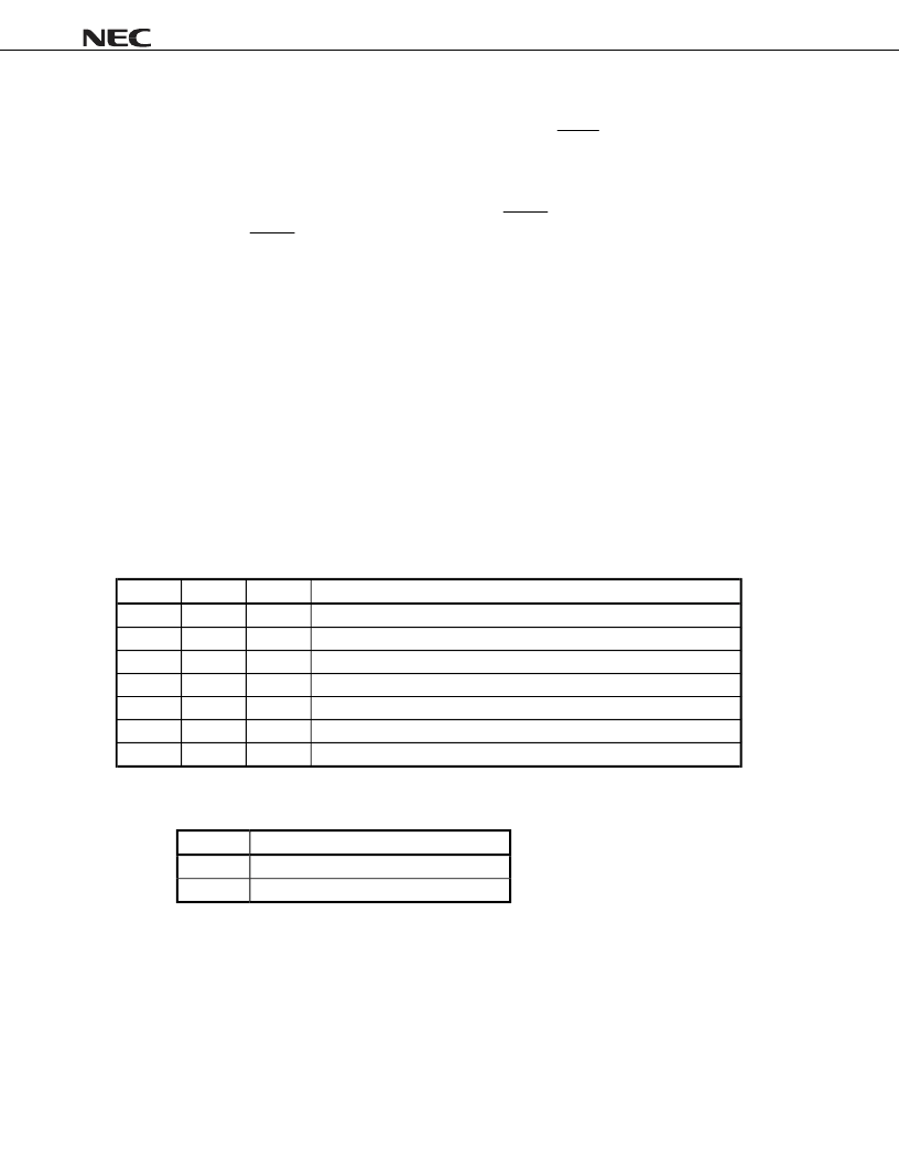
P2
P1
P0
Boot Mode
0
0
0
Non-boot
Note
0
0
1
X memory initial boot
0
1
0
Y memory initial boot
0
1
1
XY memory initial boot
1
0
0
External memory initial boot
1
0
1
Host boot
1
1
0
Serial boot
Note
This setting is used when the
μ
PD77210 Family must be reset upon restoration from standby mode after a
reset boot has been executed once.
P3
PLL lock range
0
120 to 160 MHz
1
80 to 120 MHz
5.1.1 Memory boot
The instruction code stored in data memory is transferred to the instruction RAM. Depending on the data memory
from which the instruction code is to be transferred, X memory boot (booting from the X data memory), Y memory
boot (booting from the Y data memory), XY memory boot (booting from the X and Y data memories), or external
memory boot (booting from the external data memory space) may be performed.
相關(guān)PDF資料 |
PDF描述 |
|---|---|
| UPD77210GJ-8EN | 16-BIT FIXED-POINT DIGITAL SIGNAL PROCESSOR |
| UPD77213F1-xxx-DA2 | 16-BIT FIXED-POINT DIGITAL SIGNAL PROCESSOR |
| UPD77213GJ-xxx-8EN | 16-BIT FIXED-POINT DIGITAL SIGNAL PROCESSOR |
| UPD7759 | ADPCM SPEECH SYNTHESIZER LSIs |
| UPD7759C | ADPCM SPEECH SYNTHESIZER LSIs |
相關(guān)代理商/技術(shù)參數(shù) |
參數(shù)描述 |
|---|---|
| UPD7759C | 制造商: 功能描述: 制造商:undefined 功能描述: 制造商:Panasonic Industrial Company 功能描述:IC |
| UPD780023AGB-G43-8EU-X3-A | 制造商:Renesas Electronics Corporation 功能描述: |
| UPD780023AGB-G44-8EU-E3-A | 制造商:Renesas Electronics Corporation 功能描述: |
| UPD780023AGC-107-8BS-A | 制造商:Renesas Electronics Corporation 功能描述:NECUPD780023AGC-107-8BS-A MASK ROM DEVIC |
| UPD780023AGK-C74-9ET-A | 制造商:Renesas Electronics Corporation 功能描述: |
發(fā)布緊急采購,3分鐘左右您將得到回復(fù)。