- 您現(xiàn)在的位置:買賣IC網(wǎng) > PDF目錄361592 > UPSD3254B-40T6T (意法半導(dǎo)體) Two and Three Channel Codewheels PDF資料下載
參數(shù)資料
| 型號: | UPSD3254B-40T6T |
| 廠商: | 意法半導(dǎo)體 |
| 英文描述: | Two and Three Channel Codewheels |
| 中文描述: | 閃存可編程系統(tǒng)設(shè)備與8032微控制器核心和256Kbit的SRAM |
| 文件頁數(shù): | 140/176頁 |
| 文件大?。?/td> | 1214K |
| 代理商: | UPSD3254B-40T6T |
第1頁第2頁第3頁第4頁第5頁第6頁第7頁第8頁第9頁第10頁第11頁第12頁第13頁第14頁第15頁第16頁第17頁第18頁第19頁第20頁第21頁第22頁第23頁第24頁第25頁第26頁第27頁第28頁第29頁第30頁第31頁第32頁第33頁第34頁第35頁第36頁第37頁第38頁第39頁第40頁第41頁第42頁第43頁第44頁第45頁第46頁第47頁第48頁第49頁第50頁第51頁第52頁第53頁第54頁第55頁第56頁第57頁第58頁第59頁第60頁第61頁第62頁第63頁第64頁第65頁第66頁第67頁第68頁第69頁第70頁第71頁第72頁第73頁第74頁第75頁第76頁第77頁第78頁第79頁第80頁第81頁第82頁第83頁第84頁第85頁第86頁第87頁第88頁第89頁第90頁第91頁第92頁第93頁第94頁第95頁第96頁第97頁第98頁第99頁第100頁第101頁第102頁第103頁第104頁第105頁第106頁第107頁第108頁第109頁第110頁第111頁第112頁第113頁第114頁第115頁第116頁第117頁第118頁第119頁第120頁第121頁第122頁第123頁第124頁第125頁第126頁第127頁第128頁第129頁第130頁第131頁第132頁第133頁第134頁第135頁第136頁第137頁第138頁第139頁當(dāng)前第140頁第141頁第142頁第143頁第144頁第145頁第146頁第147頁第148頁第149頁第150頁第151頁第152頁第153頁第154頁第155頁第156頁第157頁第158頁第159頁第160頁第161頁第162頁第163頁第164頁第165頁第166頁第167頁第168頁第169頁第170頁第171頁第172頁第173頁第174頁第175頁第176頁
μPSD325X DEVICES
140/176
RESET TIMING AND DEVICE STATUS AT RESET
Upon Power-up, the PSD MODULE requires a Re-
set (RESET) pulse of duration t
NLNH-PO
after V
CC
is steady. During this period, the device loads in-
ternal configurations, clears some of the registers
and sets the Flash memory into operating mode.
After the rising edge of Reset (RESET), the PSD
MODULE remains in the Reset Mode for an addi-
tional period, t
OPR
, before the first memory access
is allowed.
The Flash memory is reset to the READ Mode
upon Power-up. Sector Select (FS0-FS7 and
CSBOOT0-CSBOOT3) must all be Low, WRITE
Strobe (WR, CNTL0) High, during Power-on
RESET for maximum security of the data contents
and to remove the possibility of a byte being writ-
ten on the first edge of WRITE Strobe (WR). Any
Flash memory WRITE cycle initiation is prevented
automatically when V
CC
is below V
LKO
.
Warm RESET
Once the device is up and running, the PSD MOD-
ULE can be reset with a pulse of a much shorter
duration, t
NLNH
. The same t
OPR
period is needed
before the device is operational after a Warm
RESET. Figure 71 shows the timing of the Power-
up and Warm RESET.
I/O Pin, Register and PLD Status at RESET
Table 105 shows the I/O pin, register and PLD sta-
tus during Power-on RESET, Warm RESET, and
Power-down Mode. PLD outputs are always valid
during Warm RESET, and they are valid in Power-
on RESET once the internal Configuration bits are
loaded. This loading is completed typically long
before the V
CC
ramps up to operating level. Once
the PLD is active, the state of the outputs are de-
termined by the PLD equations.
Reset of Flash Memory Erase and Program
Cycles
A Reset (RESET) also resets the internal Flash
memory state machine. During a Flash memory
Program or Erase cycle, Reset (RESET) termi-
nates the cycle and returns the Flash memory to
the READ Mode within a period of t
NLNH-A
.
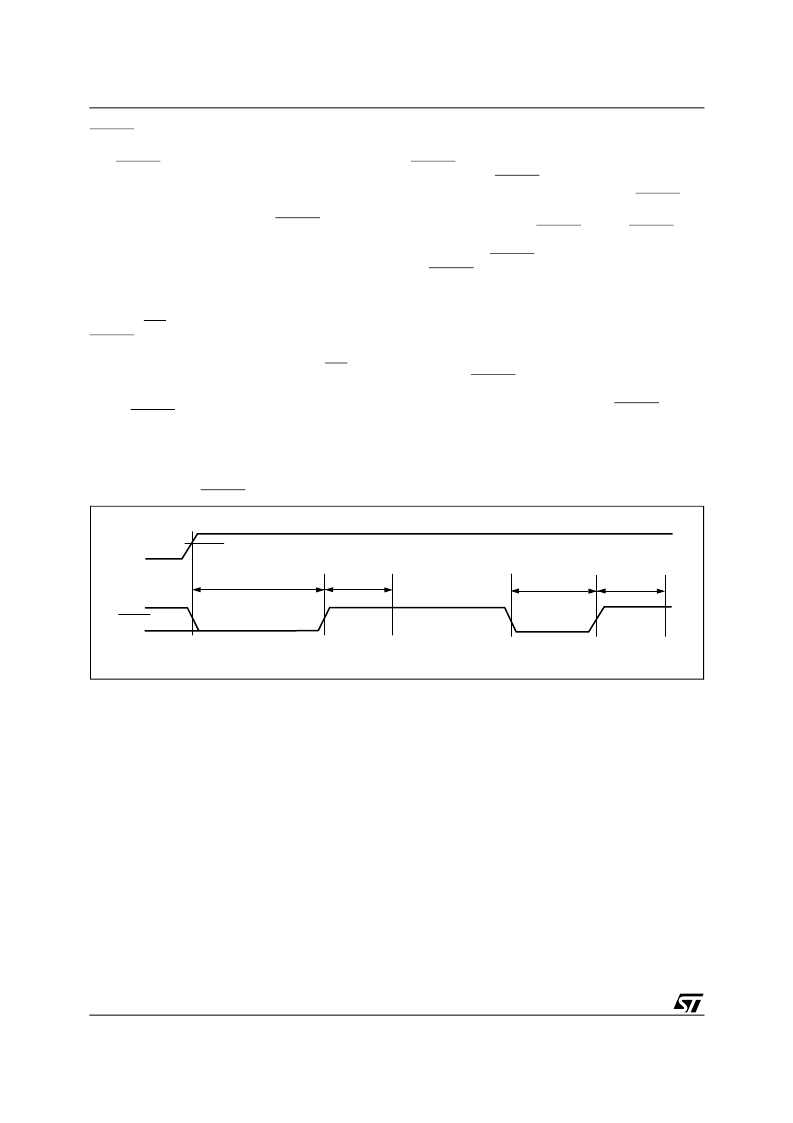
Figure 71. Reset (RESET) Timing
tNLNH-PO
Power-On Reset
tOPR
AI02866b
RESET
tNLNH
tNLNH-A
Warm Reset
tOPR
V
CC
V
CC
(min)
相關(guān)PDF資料 |
PDF描述 |
|---|---|
| UPSD3254B-40U1 | 8-bit Microcontroller with 2/4/8K Bytes In-System Programmable Flash |
| UPSD3254B-40U1T | Two and Three Channel Codewheels |
| UPSD3254B-40U6 | Flash Programmable System Devices with 8032 Microcontroller Core and 256Kbit SRAM |
| UPSD3254B-40U6T | Flash Programmable System Devices with 8032 Microcontroller Core and 256Kbit SRAM |
| UPSD3254BV-40T1 | POWERLINE: RP30-S_DE - 2:1 Wide Input Voltage Range- 30 Watts Output Power- 1.6kVDC Isolation- Fixed Operating Frequency- Six-Sided Continuous Shield- International Safety Standard Approvals- Ul 1950 Component Recognised- Standard 50.8 x40.6x10.2mm Package- Efficiency to 90% |
相關(guān)代理商/技術(shù)參數(shù) |
參數(shù)描述 |
|---|---|
| UPSD3254B-40U1 | 制造商:STMICROELECTRONICS 制造商全稱:STMicroelectronics 功能描述:Flash Programmable System Device with 8032 Microcontroller Core |
| UPSD3254B-40U1T | 制造商:STMICROELECTRONICS 制造商全稱:STMicroelectronics 功能描述:Flash Programmable System Device with 8032 Microcontroller Core |
| UPSD3254B-40U6 | 制造商:STMICROELECTRONICS 制造商全稱:STMicroelectronics 功能描述:Flash Programmable System Device with 8032 Microcontroller Core |
| UPSD3254B-40U6T | 制造商:STMICROELECTRONICS 制造商全稱:STMicroelectronics 功能描述:Flash Programmable System Device with 8032 Microcontroller Core |
| UPSD3254BV | 制造商:STMICROELECTRONICS 制造商全稱:STMicroelectronics 功能描述:Flash Programmable System Devices with 8032 Microcontroller Core |
發(fā)布緊急采購,3分鐘左右您將得到回復(fù)。