- 您現(xiàn)在的位置:買賣IC網(wǎng) > PDF目錄361639 > V350EPC-40 BUS CONTROLLER PDF資料下載
參數(shù)資料
| 型號: | V350EPC-40 |
| 英文描述: | BUS CONTROLLER |
| 中文描述: | 總線控制器 |
| 文件頁數(shù): | 10/18頁 |
| 文件大小: | 154K |
| 代理商: | V350EPC-40 |
V350EPC
10
V350EPC Data Sheet Rev 1.1
Copyright 1998, V3 Semiconductor Inc.
3.0 DC Specifications
The DC specifications for the PCI bus signals match exactly those given in the PCI Specification, Rev.
2.1, Section 4.2.1.1. For more information on the PCI DC specifications, see the PCI Specification.
3.1
PCI Bus DC Specifications
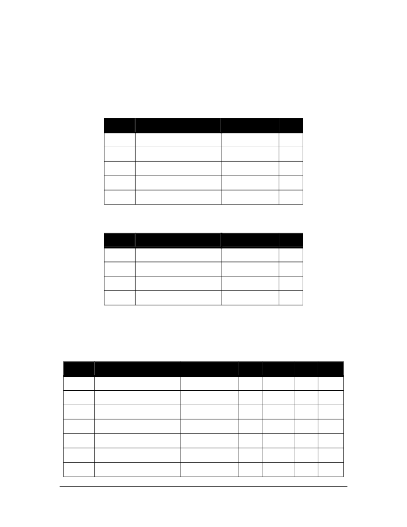
Table 6: Absolute Maximum Ratings
Symbol
Parameter
Value
Units
V
CC
Supply voltage
-0.3 to +7
V
V
IN
DC input voltage
-0.3 to V
CC
+0.3
V
I
IN
DC input current
± 10
mA
Tj
Junction temperature
125
°C
T
STG
Storage temperature range
-40 to +125
°C
Table 7: Guaranteed Operating Conditions
Symbol
Parameter
Value
Units
V
CC
Supply voltage 5 volt
4.50 to 5.50
V
V
CC
Supply voltage 3.3 volt
3.0 to 3.60
V
Theta Ja Thermal resistance
50
°C/w
T
A
Ambient temperature range
-40 to 85
°C
Table 8: PCI Bus Signals DC Operating Specifications
Symbol
Parameter
Condition
Min
Max
Units
Notes
V
IH
Input high voltage
2.0
V
CC
+0.5
V
V
IL
Input low voltage
-0.5
0.8
V
I
IH
Input high leakage current
V
IN
= 2.7V
70
μ
A
1
I
IL
Input low leakage current
V
IN
= 0.5V
-70
μ
A
1
V
OH
Output high voltage
I
OUT
= -2mA
2.4
V
V
OL
Output low voltage
I
OUT
= 3mA, 6mA
0.55
V
2
C
IN
Input pin capacitance
10
pF
3
Powered by ICminer.com Electronic-Library Service CopyRight 2003
相關PDF資料 |
PDF描述 |
|---|---|
| V350ME01-LF | VOLTAGE CONTROLLED OSCILLATOR |
| V350ME01 | FUSE 2.00A 32V FAST THIN 0402 |
| V350ME09-LF | VOLTAGE CONTROLLED OSCILLATOR |
| V35642R05KG-K50 | x64 EDO Page Mode DRAM Module |
| V35642R05KG-K60 | x64 EDO Page Mode DRAM Module |
相關代理商/技術參數(shù) |
參數(shù)描述 |
|---|---|
| V350K10 | 制造商:未知廠家 制造商全稱:未知廠家 功能描述: |
| V350K14 | 制造商:未知廠家 制造商全稱:未知廠家 功能描述: |
| V350K20 | 制造商:未知廠家 制造商全稱:未知廠家 功能描述: |
| V350K5 | 制造商:未知廠家 制造商全稱:未知廠家 功能描述: |
| V350K7 | 制造商:未知廠家 制造商全稱:未知廠家 功能描述: |
發(fā)布緊急采購,3分鐘左右您將得到回復。