- 您現(xiàn)在的位置:買賣IC網(wǎng) > PDF目錄359352 > VCH16373ADGG (NXP SEMICONDUCTORS) 16-bit D-type transparent latch with 5 Volt tolerant inputs/outputs 3-State PDF資料下載
參數(shù)資料
| 型號: | VCH16373ADGG |
| 廠商: | NXP SEMICONDUCTORS |
| 元件分類: | 通用總線功能 |
| 英文描述: | 16-bit D-type transparent latch with 5 Volt tolerant inputs/outputs 3-State |
| 中文描述: | LVC/LCX/Z SERIES, DUAL 8-BIT DRIVER, TRUE OUTPUT, PDSO48 |
| 文件頁數(shù): | 6/10頁 |
| 文件大小: | 83K |
| 代理商: | VCH16373ADGG |
Philips Semiconductors
Product specification
74LVC16373A/
74LVCH16373A
16-bit D-type transparent latch with 5 Volt tolerant
inputs/outputs (3-State)
1998 Mar 17
6
DC ELECTRICAL CHARACTERISTICS (Continued)
Over recommended operating conditions voltages are referenced to GND (ground = 0V)
LIMITS
SYMBOL
PARAMETER
TEST CONDITIONS
Temp = -40
°
C to +85
°
C
TYP
1
UNIT
MIN
MAX
I
BHL
I
BHH
I
BHLO
I
BHHO
Bus hold LOW sustaining current
V
CC
= 3.0V; V
I
= 0.8V
2, 3, 4
V
CC
= 3.0V; V
I
= 2.0V
2, 3, 4
V
CC
= 3.6V
2, 3, 5
V
CC
= 3.6V
2, 3, 5
75
μ
A
μ
A
μ
A
μ
A
Bus hold HIGH sustaining current
–75
Bus hold LOW overdrive current
500
Bus hold HIGH overdrive current
–500
NOTES:
1. All typical values are at V
CC
= 3.3V and T
amb
= 25
°
C.
2. Valid for data inputs of bus hold parts (LVCH16-A) only.
3. For data inputs only, control inputs do not have a bus hold circuit.
4. The specified sustaining current at the data input holds the input below the specified V
level.
5. The specified overdrive current at the data input forces the data input to the opposite logic input state.
6. For bus hold parts, the bus hold circuit is switched off when V
i
exceeds V
CC
allowing 5.5V on the input terminal.
AC CHARACTERISTICS
GND = 0V; t
R
= t
F
= 2.5ns; C
L
= 50pF; R
L
= 500
; T
amb
= –40
°
C to +85
°
C.
LIMITS
SYMBOL
PARAMETER
WAVEFORM
V
CC
= 3.3V
±
0.3V
TYP
1
V
CC
= 2.7V
V
CC
= 1.2V
UNIT
MIN
MAX
MIN
MAX
TYP
t
PHL
t
PLH
Propagation delay
Dn to Qn
1, 5
1.5
3.0
4.7
1.5
5.7
12
ns
t
PHL
t
PLH
Propagation delay
LE to Qn
2, 5
1.5
3.4
4.8
1.5
5.8
14
ns
t
PZH
t
PZL
3-State output enable time
OE to Qn
4, 5
1.5
3.5
5.5
1.5
6.5
18
ns
t
PHZ
t
PLZ
3-State output disable time
OE to Qn
4, 5
1.5
3.9
5.4
1.5
6.4
11
ns
t
W
LE pulse width HIGH
2
3
2.0
–
3
–
–
ns
t
su
Set-up time Dn to LE
3
1.7
–0.1
–
1.7
–
–
ns
t
h
Hold time Dn to LE
3
1.2
0.1
–
1.2
–
–
ns
NOTE:
1. All typical values are at V
CC
= 3.3V and T
amb
= 25
°
C.
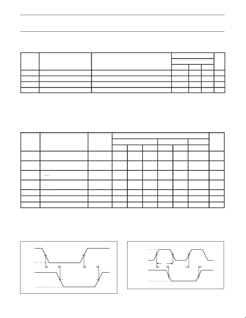
AC WAVEFORMS
V
M
= 1.5V at V
CC
V
OL
and V
OH
are the typical output voltage drop that occur with the output load.
V
X
= V
OL
+ 0.3V at V
CC
2.7V; V
X
= V
OL
+ 0.1 V
CC
at V
CC
V
Y
= V
OH
–0.3V at V
CC
2.7V; V
Y
= V
OH
– 0.1 V
CC
at V
CC
2.7V; V
M
= 0.5 V
CC
at V
CC
2.7V.
2.7V
2.7V
SW00070
Dn INPUT
V
M
t
PHL
t
PLH
V
OL
V
I
V
M
GND
V
OH
Qn OUTPUT
V
M
Waveform 1. Input (Dn) to output (Qn) propagation delays
V
M
V
M
V
M
V
M
t
w
t
PHL
t
PLH
LE INPUT
Qn OUTPUT
SW00071
V
I
GND
V
OH
V
OL
V
M
Waveform 2. Latch enable input (LE) pulse width, the latch
enable input to output (Qn) propagation delays
相關(guān)PDF資料 |
PDF描述 |
|---|---|
| VCH16373ADL | 16-bit D-type transparent latch with 5 Volt tolerant inputs/outputs 3-State |
| VCH16374ADGG | 16-bit edge triggered D-type flip-flop with 5 Volt tolerant inputs/outputs 3-State |
| VCH16374ADL | 16-bit edge triggered D-type flip-flop with 5 Volt tolerant inputs/outputs 3-State |
| VCH16541ADGG | 16-bit buffer/line driver 3-State |
| VCH16541ADL | 16-bit buffer/line driver 3-State |
相關(guān)代理商/技術(shù)參數(shù) |
參數(shù)描述 |
|---|---|
| VCH16373ADL | 制造商:PHILIPS 制造商全稱:NXP Semiconductors 功能描述:16-bit D-type transparent latch with 5 Volt tolerant inputs/outputs 3-State |
| VCH16374ADGG | 制造商:PHILIPS 制造商全稱:NXP Semiconductors 功能描述:16-bit edge triggered D-type flip-flop with 5 Volt tolerant inputs/outputs 3-State |
| VCH16374ADL | 制造商:PHILIPS 制造商全稱:NXP Semiconductors 功能描述:16-bit edge triggered D-type flip-flop with 5 Volt tolerant inputs/outputs 3-State |
| VCH16541ADGG | 制造商:PHILIPS 制造商全稱:NXP Semiconductors 功能描述:16-bit buffer/line driver 3-State |
| VCH16541ADL | 制造商:PHILIPS 制造商全稱:NXP Semiconductors 功能描述:16-bit buffer/line driver 3-State |
發(fā)布緊急采購,3分鐘左右您將得到回復(fù)。