- 您現(xiàn)在的位置:買賣IC網(wǎng) > PDF目錄202514 > VKB51B2-51.84MHZ (CONNOR WINFIELD CORP) VCXO, CLOCK, 51.84 MHz, HCMOS OUTPUT PDF資料下載
參數(shù)資料
| 型號(hào): | VKB51B2-51.84MHZ |
| 廠商: | CONNOR WINFIELD CORP |
| 元件分類: | VCXO, clock |
| 英文描述: | VCXO, CLOCK, 51.84 MHz, HCMOS OUTPUT |
| 封裝: | HERMETICALLY SEALED, CERAMIC, LCC-6 |
| 文件頁數(shù): | 2/2頁 |
| 文件大小: | 74K |
| 代理商: | VKB51B2-51.84MHZ |

E/D
N/C
POWER
SUPPLY
A
V
OSC
INPUT for C/V
.01uf
OSCILLOSCOPE
FREQ
COUNTER
PROBE
CL
1 2
3
65
4
7.48 DIA
(190mm)
.69
(17.5mm)
.315
(8.0mm)
.039 R
(1.0mm)
.826 DIA
(21mm)
.511 DIA
(13mm)
9.84 DIA
(250mm)
MEETS EIA—481A and EIAJ—1009B
2,000 PCS/REEL
120
.08
(2.0mm)
3.15
(8.0mm)
.08
(2.0mm)
.157
(4.0mm)
.06 DIA
(1.5mm)
.31
(7.9mm)
.21
(5.4mm)
PIN 1
.295 (7.5mm)
.07 (1.75mm)
.63 (16.0mm)
Specifications subject to change without notice. All dimensions in inches. Copyright 1998 The Connor-Winfield Corporation
2111 Comprehensive Drive
Aurora, Illinois 60505
Phone: 630- 851- 4722
Fax: 630- 851- 5040
www.conwin.com
Package Characteristics
Package
Hermetically sealed, ceramic leadless package.
Bulletin
Vx265
Page
2 of 2
Revision
08
Date
16 Dec 2003
Soldering
General Conditions
260°C max x 10 sec max x 2 times max or
230°C max x 180 sec max x 1 time
Typical Operation Data
20 to 100 sec up to 215°C, 50 sec at 215°C,
(Vapor phase reflow)
then down to room temperature per 1 to 5°C / sec
Environmental Characteristics
Temperature Cycle
The specimen shall meet electrical characteristics after
tested 5 cycles of -55°C / 30 minutes and +125°C / 30 minutes
Hermetical
No bubbles appear in Flourinert (FC-43) at 125°C ±5°C for 5 minutes
Solvent Resistance
Marking will withstand immersion in
Isopropyl Alcohol or Trichloroethylene
Mechanical Characteristics
Free Drop
The specimen shall meet electrical characteristics after tested 3 times,
Free Drop testing on the hard wooden board from a height of 75 cm.
Vibration
The specimen shall meet electrical characteristics after tested
by the following conditions: 10-55Hz 1.5mm Amplitude,
55-2000 Hz 20 G's, 2 hours for each plane
Thermal Shock
After applied Thermal Shock of
245°C max x 10 sec max x 2 times, or 215°C max x 180 sec max,
the specimen shall meet electrical characteristics
Solderability
(EIAJ-RCX-0102/101 Condition 1a)
1) Flux: MIL-F-14256 (WW Rosin=25%, Isopropyl Alcohol = 75%)
2) Solder: QQ-S-571 (Sn = 63%, Pb = 37%)
3) Solder bath temperature: 235°C ±5°C
4) Depth of immersion: Up to electrical terminal
5) Immersing time: Within 2 sec ±0.5 sec into solder bath
After performing the above procedures, a newly soldered coverage shall be greater than 90%
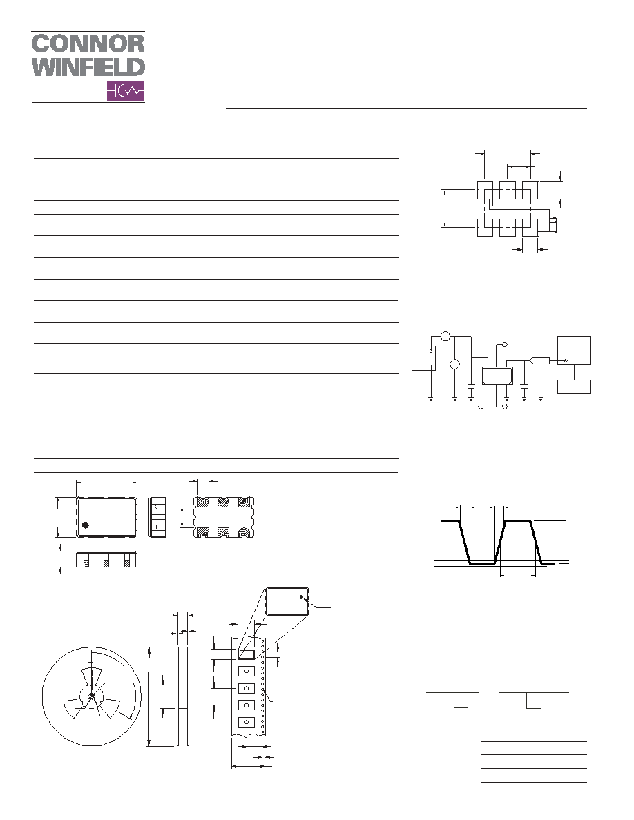
Pin Function
1: Control Voltage
2: Tri-state Enable /Disable
3: Ground
4: Output
5: N/C
6: VDD
Suggested Pad Layout
Test Circuit
Output Waveform
Ordering Information
VKB51B2 - 51.84 MHz
VCXO
SERIES
CENTER
FREQUENCY
Tape and Reel Dimensions
.295 MAX
(7.5mm)
.079 MAX
(2.0mm)
0.102
(2.6mm)
.197 MAX
(5.0mm)
0.055
(1.4mm)
Dimensional ±.02" (±0.5mm)
Tolerance:
±.008" (±0.2mm)
#1
#2
#3
#6
#5
#4
#1
#2
#3
#6
#5
#4
Dimensional
Tolerance:
±.02" (.508mm)
±.005" (.127mm)
Bypass capacitor, C–by, should be
ceramic capacitor
≥ .01uf.
0.165
(4.2mm)
VDD
GROUND
C–by
0.200
(5.08mm)
0.100
(2.54mm)
0.079
(2.0mm)
0.070
(1.8mm)
SYMMETRY
"1" LEVEL
"0" LEVEL
+2.64Vdc
+1.65Vdc
+0.66Vdc
0.0Vdc
TR
TF
80% Vcc
50% Vcc
20% Vcc
相關(guān)PDF資料 |
PDF描述 |
|---|---|
| VKB62B2-16.384MHZ | VCXO, CLOCK, 16.384 MHz, HCMOS OUTPUT |
| VKB62B2-FREQ-OUT27 | VCXO, CLOCK, 1 MHz - 45 MHz, HCMOS OUTPUT |
| VKP100MT315-(6)C | 3-OUTPUT 100 W DC-DC REG PWR SUPPLY MODULE |
| VKP60LT315 | 3-OUTPUT 60 W DC-DC REG PWR SUPPLY MODULE |
| VKP60MT315 | 3-OUTPUT 60 W DC-DC REG PWR SUPPLY MODULE |
相關(guān)代理商/技術(shù)參數(shù) |
參數(shù)描述 |
|---|---|
| VKBAA80C-00000-000 | 制造商:Carling Technologies 功能描述:V-SERIES ROCKER SWITCH - Bulk |
| VKBAA80H-CMH00-000 | 制造商:Carling Technologies 功能描述:V-SERIES ROCKER SWITCH - Bulk |
| VKBAAD0C-00000-000 | 制造商:Carling Technologies 功能描述:V-SERIES ROCKER SWITCH - Bulk |
| VKBAAJ0B-00000-000 | 制造商:Carling Technologies 功能描述:V-SERIES ROCKER SWITCH - Bulk |
| VKBAAP0C-00000-000 | 制造商:Carling Technologies 功能描述:V-SERIES ROCKER SWITCH - Bulk |
發(fā)布緊急采購,3分鐘左右您將得到回復(fù)。