- 您現(xiàn)在的位置:買賣IC網(wǎng) > PDF目錄359420 > VRE410AS Analog IC PDF資料下載
參數(shù)資料
| 型號(hào): | VRE410AS |
| 英文描述: | Analog IC |
| 中文描述: | 模擬IC |
| 文件頁(yè)數(shù): | 4/5頁(yè) |
| 文件大小: | 404K |
| 代理商: | VRE410AS |
DISCUSSION OF PERFORMANCE
VRE410DS REV. A MAY 1996
VRE410
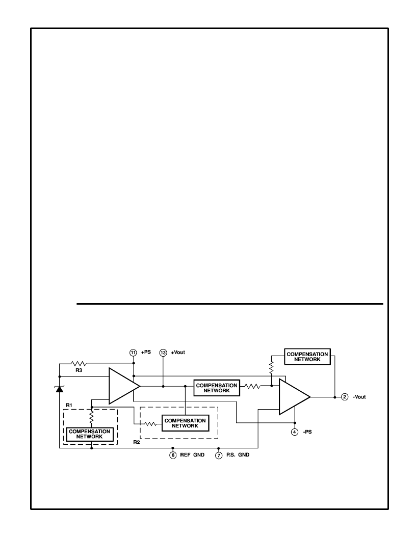
FIGURE 2
THEORY OF OPERATION
The following discussion refers to the schematic
below. In operation, approximately 6.3 volts is
applied to the noninverting input of the op amp. The
voltage is amplified by the op amp to produce a
10.000V output. The gain is determined by the
networks R1 and R2: G=1 + R2/R1. The 6.3V zener
diode is used because it is the most stable diode
over time and temperature.
The zener operating current is derived from the
regulated output voltage through R3. This feedback
arrangement provides a closely regulated zener
current. This current determines the slope of the
references' voltage vs. temperature function. By
trimming the zener current a lower drift over
temperature can be achieved. But since the voltage
vs.
temperature
function
compensation technique is not well suited for wide
temperature ranges.
Thaler Corporation has developed a nonlinear
compensation network of thermistors and resistors
that is used in the VRE series voltage references.
This proprietary network eliminates most of the
nonlinearity in the voltage vs. temperature function.
By then adjusting the slope, Thaler Corporation
produces a very stable voltage over wide
temperature ranges.
is
nonlinear
this
The VRE400 series voltage references have the
ground terminal brought out on two pins (pin 6 and 7)
which are connected together internally. This allows
the user to achieve greater accuracy when using a
socket. Voltage references have a voltage drop
across their power supply ground pin due to
quiescent current flowing through the contact
resistance. If the contact resistance was constant
with time and temperature, this voltage drop could be
trimmed out. When the reference is plugged into a
socket, this source of error can be as high as 20ppm.
By connecting pin 7 to the power supply ground and
pin 6 to a high impedance ground point in the
measurement circuit, the error due to the contact
resistance can be eliminated. If the unit is soldered
into place the contact resistance is sufficiently small
that it doesn't effect performance.
相關(guān)PDF資料 |
PDF描述 |
|---|---|
| VRE410AD | Analog IC |
| VRE4110K | Low Cost, SOIC-8 Precision References |
| VRPB-06B | NON-ISOLATED DC/DC CONVERTERS 5V Input / 1.5 - 3.3V Output / 6A |
| VRPB-06F1A0 | NON-ISOLATED DC/DC CONVERTERS |
| VRPB-06F33H | NON-ISOLATED DC/DC CONVERTERS |
相關(guān)代理商/技術(shù)參數(shù) |
參數(shù)描述 |
|---|---|
| VRE410B | 制造商:未知廠家 制造商全稱:未知廠家 功能描述:Precision Dual Reference |
| VRE410BD | 制造商:未知廠家 制造商全稱:未知廠家 功能描述:Analog IC |
| VRE410BS | 功能描述:基準(zhǔn)電壓& 基準(zhǔn)電流 Ref. +/-10V, 0/70C 1ppm RoHS:否 制造商:STMicroelectronics 產(chǎn)品:Voltage References 拓?fù)浣Y(jié)構(gòu):Shunt References 參考類型:Programmable 輸出電壓:1.24 V to 18 V 初始準(zhǔn)確度:0.25 % 平均溫度系數(shù)(典型值):100 PPM / C 串聯(lián) VREF - 輸入電壓(最大值): 串聯(lián) VREF - 輸入電壓(最小值): 分流電流(最大值):60 mA 最大工作溫度:+ 125 C 封裝 / 箱體:SOT-23-3L 封裝:Reel |
| VRE410C | 制造商:未知廠家 制造商全稱:未知廠家 功能描述:Precision Dual Reference |
| VRE410CD | 制造商:未知廠家 制造商全稱:未知廠家 功能描述:Analog IC |
發(fā)布緊急采購(gòu),3分鐘左右您將得到回復(fù)。