- 您現(xiàn)在的位置:買賣IC網(wǎng) > PDF目錄359427 > VSC3144 (Vitesse Semiconductor Corporation.) 6.5 Gbps 144 】 144 Asynchronous Crosspoint Switch PDF資料下載
參數(shù)資料
| 型號: | VSC3144 |
| 廠商: | Vitesse Semiconductor Corporation. |
| 英文描述: | 6.5 Gbps 144 】 144 Asynchronous Crosspoint Switch |
| 中文描述: | 6.5 Gbps的144】144異步交叉點開關 |
| 文件頁數(shù): | 2/2頁 |
| 文件大小: | 473K |
| 代理商: | VSC3144 |
Trademarks
TM
Vitesse, ASIC-Friendly, FibreTimer, TimeStream, Snoop Loop, Super FEC, FOCUSConnect, Meigs-II, Meigs-IIe, Lansing, Campbell-I, Barrington,
PaceMaker, HOVCAT48, HOVCAT48e, HOVCAT192, HOVCAT192e, Micro PHY, FOCUS32, FOCUS16, IQ2200, NexSAS, VersaCAT, GigaStream, HawX,
SparX, StaX, VstaX, SimpliPHY,VeriPHY, ActiPHY, XFP PRO, SFP PRO, Smart-LINK, OctalMAC, EQ Technology are trademarks in the United States and/or
other jurisdictions of Vitesse Semiconductor Corporation. All other trademarks or registered trademarks mentioned herein are the property of their respective
holders.
Vitesse Semiconductor Corporation (“Vitesse”) retains the right to make changes to its products or specifications to improve performance, reliability or
manufacturability. All information in this document, including descriptions of features, functions, performance, technical specifications and availability, is
subject to change without notice at any time. While the information furnished herein is held to be accurate and reliable, no responsibility will be assumed by
Vitesse for its use. Furthermore, the information contained herein does not convey to the purchaser of microelectronic devices any license under the patent
right of any manufacturer.
Copyright 2006
741 Calle Plano
Camarillo, CA 93012, USA
Tel: +1 805.388.3700
Fax: +1 805.987.5896
www.vitesse.com
sales@vitesse.com
VSC3144
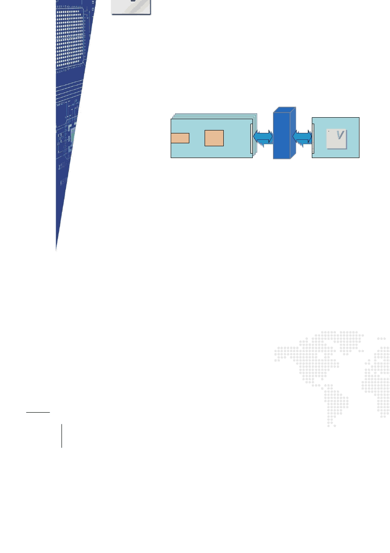
Line Cards
FPGA/
ASIC
OE
BACK PL ANE APPL ICATION:
B
a
c
k
p
l
a
n
e
VSC3144
Central Switch
GE NE R AL DE S CR IPTION:
S PE CIF ICATIONS :
programmed to connect to any of its inputs. The
signal path through the device uses no registers and
is fully asynchronous. This means there are no restrictions on the phase,
frequency, or signal pattern of any input.
A high degree of signal integrity is maintained throughout the VSC3144
device because each high-speed output is a fully differential,
switched-current driver with on-die termnations. Data inputs are
termnated on-die using 100 resistors between true and complement
inputs, with a common connection to an internal bias source, which
facilitates AC coupling to the switch inputs.
Core programmng for the VSC3144 device can be sequential on a
port-by-port basis, or multiple programassignments can be queued and
issued simultaneously using the CONFIG bit. The entire device can be
initialized for straight-through, multicast, or other configurations. Unused
channels can be powered down to allow efficient use of the switch in
applications that require only a subset of the available I/O channels.
Power-down is enabled in the software by programmng individual unused
outputs with a power-down code.
`
6.5 Gbps NRZ per-channel data rate
`
2.5 V power supply (2.5 V or 3.3 V programport power supply)
`
2.5 V or 3.3 V CMOS TTL-compatible I/O
`
Differential CML I/O with integrated termnation impedance
`
0
°C to 85
°C operating temperature range
相關PDF資料 |
PDF描述 |
|---|---|
| VSC3172 | 6.5 Gbps 72 】 72 Asynchronous Crosspoint Switch |
| VSC3208 | 4, 8 and 12 Port 155 Mbps to 4.25 Gbps Crosspoint Switches with CDR |
| VSC3304 | 8.5 Gbps 4 】 4 Crosspoint Switch |
| VSC3312 | 6.5 Gbps 12x12 Crosspoint Switch |
| VSC5529 | 9.9 Gb/s - 12.5 Gb/s NRZ LiNbO3 Modulator Driver |
相關代理商/技術參數(shù) |
參數(shù)描述 |
|---|---|
| VSC3144XHR | 制造商:Vitesse Semiconductor Corporation 功能描述:CHIPSET |
| VSC3144XHR-30 | 制造商:Vitesse Semiconductor Corporation 功能描述:IC CHIP |
| VSC3172 | 制造商:VITESSE 制造商全稱:Vitesse Semiconductor Corporation 功能描述:6.5 Gbps 72 】 72 Asynchronous Crosspoint Switch |
| VSC3204 | 制造商:VITESSE 制造商全稱:Vitesse Semiconductor Corporation 功能描述:4, 8 and 12 Port 155 Mbps to 4.25 Gbps Crosspoint Switches with CDR |
| VSC3208 | 制造商:VITESSE 制造商全稱:Vitesse Semiconductor Corporation 功能描述:4, 8 and 12 Port 155 Mbps to 4.25 Gbps Crosspoint Switches with CDR |
發(fā)布緊急采購,3分鐘左右您將得到回復。