- 您現(xiàn)在的位置:買賣IC網(wǎng) > PDF目錄203610 > VV-701-DAT-2EAE-20M4800000 (VECTRON INTERNATIONAL) VCXO, CLOCK, 20.48 MHz, CMOS OUTPUT PDF資料下載
參數(shù)資料
| 型號(hào): | VV-701-DAT-2EAE-20M4800000 |
| 廠商: | VECTRON INTERNATIONAL |
| 元件分類: | VCXO, clock |
| 英文描述: | VCXO, CLOCK, 20.48 MHz, CMOS OUTPUT |
| 封裝: | ROHS COMPLIANT, HERMETIC SEALED PACKAGE-6 |
| 文件頁(yè)數(shù): | 3/6頁(yè) |
| 文件大小: | 202K |
| 代理商: | VV-701-DAT-2EAE-20M4800000 |
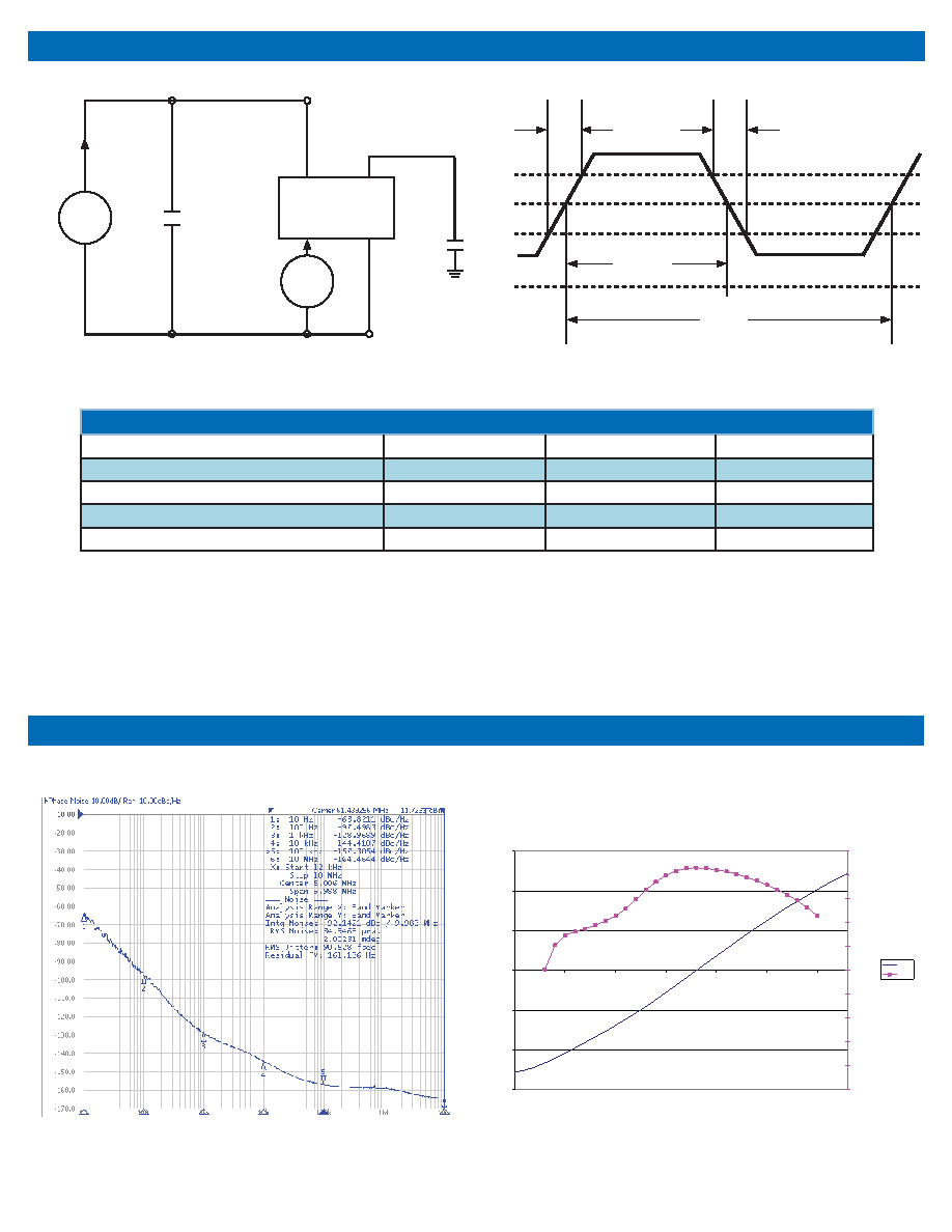
Table 2. Absolute Maximum Ratings
Parameter
Symbol
Ratings
Unit
Power Supply
V
CC
0 to 6
V
Voltage Control Range
V
C
0 to V
CC
V
Storage Temperature
TS
-55 to 125
°C
Soldering Temp/Time
T
LS
260 / 20
°C / sec
Stresses in excess of the absolute maximum ratings can permanently damage the device. Functional operation is not implied at these or
any other conditions in excess of conditions represented in the operational sections of this datasheet. Exposure to absolute maximum
ratings for extended periods may adversely affect device reliability. Permanent damage is also possible if OD or Vc is applied before Vcc.
Typical Phase Noise
Typical Gain
VV-701 @ 61.44 MHz
-150
-100
-50
0
50
100
150
0
0.5
1
1.5
2
2.5
3
Vc (volts)
Pull
(ppm)
0
10
20
30
40
50
60
70
80
90
100
Gain
(ppm/V)
Pull
Gain
Test Circuit
Waveform
Fig 1: Test Circuit
Fig 2: Output Waveform
t
R
t
F
0.8*V
DD
0.1*V
DD
50%
On Time
Period
I
DD
V
DD
V
C
I
C
15pF
6
13
4
.1μF
+
-
+
-
Page3
Vectron International 267 Lowell Road, Hudson, NH 03051 Tel: 1-88-VECTRON-1 http://www.vectron.com
發(fā)布緊急采購(gòu),3分鐘左右您將得到回復(fù)。