- 您現(xiàn)在的位置:買賣IC網(wǎng) > PDF目錄203626 > W332M72V-125SBC (WHITE ELECTRONIC DESIGNS CORP) 32M X 72 SYNCHRONOUS DRAM, 6 ns, PBGA208 PDF資料下載
參數(shù)資料
| 型號(hào): | W332M72V-125SBC |
| 廠商: | WHITE ELECTRONIC DESIGNS CORP |
| 元件分類: | DRAM |
| 英文描述: | 32M X 72 SYNCHRONOUS DRAM, 6 ns, PBGA208 |
| 封裝: | 16 X 22 MM, PLASTIC, BGA-208 |
| 文件頁數(shù): | 12/15頁 |
| 文件大小: | 257K |
| 代理商: | W332M72V-125SBC |
6
White Electronic Designs
W332M72V-XBX
March 2006
Rev. 3
White Electronic Designs Corporation (602) 437-1520 www.wedc.com
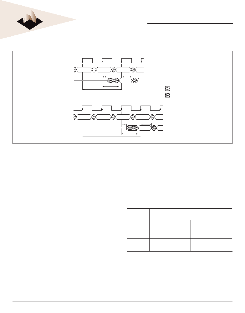
FIGURE 4 – CAS LATENCY
OPERATING MODE
The normal operating mode is selected by setting M7and
M8 to zero; the other combinations of values for M7 and
M8 are reserved for future use and/or test modes. The
programmed burst length applies to both READ and
WRITE bursts.
Test modes and reserved states should not be used
because unknown operation or incompatibility with future
versions may result.
TABLE 2 – CAS LATENCY
SPEED
ALLOWABLE OPERATING
FREQUENCY (MHz)
CAS
LATENCY = 2
CAS
LATENCY = 3
-100
≤ 75
≤ 100
-125
≤ 100
≤ 125
-133
≤ 100
≤ 133
WRITE BURST MODE
When M9 = 0, the burst length programmed via M0-M2
applies to both READ and WRITE bursts; when M9 = 1,
the programmed burst length applies to READ bursts, but
write accesses are single-location (nonburst) accesses.
CLK
Command
I/O
CLK
Command
I/O
T0
T1
T2
T3
T0
T1
T2
T3
T4
READ
NOP
CAS Latency = 2
DOUT
tLZ
tOH
tAC
READ
NOP
DOUT
tLZ
tOH
tAC
CAS Latency = 3
DON'T CARE
UNDEFINED
BURST TYPE
Accesses within a given burst may be programmed to be
either sequential or interleaved; this is referred to as the
burst type and is selected via bit M3.
The ordering of accesses within a burst is determined by
the burst length, the burst type and the starting column
address, as shown in Table 1.
CAS LATENCY
The CAS latency is the delay, in clock cycles, between
the registration of a READ command and the availability
of the rst piece of output data. The latency can be set to
two or three clocks.
If a READ command is registered at clock edge n, and the
latency is m clocks, the data will be available by clock edge
n+m. The I/Os will start driving as a result of the clock
edge one cycle earlier (n + m - 1), and provided that the
relevant access times are met, the data will be valid by
clock edge n + m. For example, assuming that the clock
cycle time is such that all relevant access times are met,
if a READ command is registered at T0 and the latency
is programmed to two clocks, the I/Os will start driving
after T1 and the data will be valid by T2. Table 2 below
indicates the operating frequencies at which each CAS
latency setting can be used.
Reserved states should not be used as unknown operation
or incompatibility with future versions may result.
相關(guān)PDF資料 |
PDF描述 |
|---|---|
| W332M72V-100SBC | 32M X 72 SYNCHRONOUS DRAM, 7 ns, PBGA208 |
| W332M72V-100SBM | 32M X 72 SYNCHRONOUS DRAM, 7 ns, PBGA208 |
| W3481136G | 36 CONTACT(S), FEMALE, STRAIGHT TWO PART BOARD CONNECTOR, SOLDER, SOCKET |
| W3481136T | 36 CONTACT(S), FEMALE, STRAIGHT TWO PART BOARD CONNECTOR, SOLDER, SOCKET |
| W3481172G | 72 CONTACT(S), FEMALE, STRAIGHT TWO PART BOARD CONNECTOR, SOLDER, SOCKET |
相關(guān)代理商/技術(shù)參數(shù) |
參數(shù)描述 |
|---|---|
| W332M72V-125SBI | 制造商:Microsemi Corporation 功能描述:32M X 72 SDRAM, 3.3V, 125MHZ, 208 PBGA, INDUSTRIAL TEMP. - Bulk |
| W332M72V-125SBM | 制造商:Microsemi Corporation 功能描述:32M X 72 SDRAM, 3.3V, 125MHZ, 208 PBGA, MIL-TEMP. - Bulk 制造商:Microsemi Corporation 功能描述:SDRAM MEMORY |
| W332M72V-133BC | 制造商:Microsemi Corporation 功能描述:32M X 72 SDRAM, 3.3V, 133MHZ, 219 PBGA, COMMERCIAL TEMP. - Bulk |
| W332M72V-133BI | 制造商:Microsemi Corporation 功能描述:32M X 72 SDRAM, 3.3V, 133MHZ, 219 PBGA, INDUSTRIAL TEMP. - Bulk |
| W332M72V-133BM | 制造商:Microsemi Corporation 功能描述:32M X 72 SDRAM, 3.3V, 133MHZ, 219 PBGA, MIL-TEMP. - Bulk |
發(fā)布緊急采購,3分鐘左右您將得到回復(fù)。