- 您現(xiàn)在的位置:買賣IC網(wǎng) > PDF目錄245690 > W3E64M72S-200BI (MICROSEMI CORP-PMG MICROELECTRONICS) 64M X 72 SYNCHRONOUS DRAM, 0.8 ns, PBGA219 PDF資料下載
參數(shù)資料
| 型號(hào): | W3E64M72S-200BI |
| 廠商: | MICROSEMI CORP-PMG MICROELECTRONICS |
| 元件分類: | DRAM |
| 英文描述: | 64M X 72 SYNCHRONOUS DRAM, 0.8 ns, PBGA219 |
| 封裝: | 25 X 32 MM, PLASTIC, BGA-219 |
| 文件頁數(shù): | 6/19頁 |
| 文件大小: | 674K |
| 代理商: | W3E64M72S-200BI |
W3E64M72S-XBX
14
White Electronic Designs Corporation (602) 437-1520 www.wedc.com
White Electronic Designs
June 2005
Rev. 0
ADVANCED
White Electronic Designs Corp. reserves the right to change products or specications without notice.
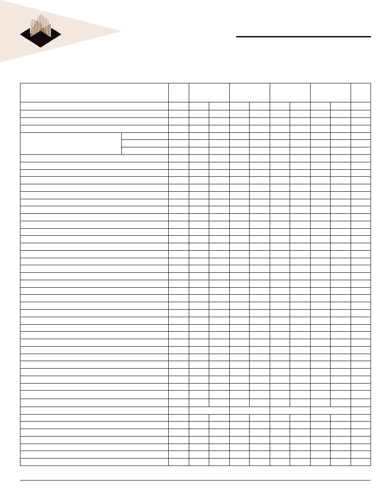
ELECTRICAL CHARACTERISTICS AND RECOMMENDED AC OPERATING CHARACTERISTICS
Notes 1-5, 14-17, 33
333 Mbs CL3/CL2.5
(53)
266 Mbs CL2.5
200 CL2
250 Mbs CL2.5
200 Mbs CL2
200 Mbs CL2.5
150 Mbs CL2
Parameter
Symbol
Min
Max
Min
Max
Min
Max
Min
Max
Units
Access window of DQs from CK/CK#
tAC
-0.70
+0.70
-0.75
+0.75
-0.8
+0.8
-0.8
+0.8
ns
CK high-level width (30)
tCH
0.45
0.55
0.45
0.55
0.45
0.55
0.45
0.55
tCK
CK low-level width (30)
tCL
0.45
0.55
0.45
0.55
0.45
0.55
0.45
0.55
tCK
Clock cycle time
CL = 3 (45, 51)
tCK (3)
6
13
ns
CL = 2.5 (45, 51)
tCK (2.5)
7.5
13
7.5
13
8
13
10
13
ns
CL = 2 (45, 51)
tCK (2)
1013101310131315
ns
DQ and DM input hold time relative to DQS (26, 31)
tDH
0.45
0.5
0.6
ns
DQ and DM input setup time relative to DQS (26, 31)
tDS
0.45
0.5
0.6
ns
DQ and DM input pulse width (for each input) (31)
tDIPW
1.75
2
ns
Access window of DQS from CK/CK#
tDQSCK
-0.6
+0.6
-0.75
+0.75
-0.8
+0.8
-0.8
+0.8
ns
DQS input high pulse width
tDQSH
0.35
tCK
DQS input low pulse width
tDQSL
0.35
tCK
DQS-DQ skew, DQS to last DQ valid, per group, per access (25, 26)
tDQSQ
0.45
0.5
0.6
ns
Write command to rst DQS latching transition
tDQSS
0.75
1.25
0.75
1.25
0.75
1.25
0.75
1.25
tCK
DQS falling edge to CK rising - setup time
tDSS
0.2
tCK
DQS falling edge from CK rising - hold time
tDSH
0.2
tCK
Half clock period (34)
tHP
tCH,tCL
ns
Data-out high-impedance window from CK/CK# (18, 42)
tHZ
+0.70
+0.75
+0.8
ns
Data-out low-impedance window from CK/CK# (18, 42)
tLZ
-0.70
-0.75
-0.8
ns
Address and control input hold time (fast slew rate)
tIH
F
0.75
0.90
1.1
ns
Address and control input setup time (fast slew rate)
tIS
F
0.75
0.90
1.1
ns
Address and control input hold time (slow slew rate) (14)
tIH
S
0.8
1
1.1
ns
Address and control input setup time (slow slew rate) (14)
tIS
S
0.8
1
1.1
ns
LOAD MODE REGISTER command cycle time
tMRD
12
15
16
ns
DQ-DQS hold, DQS to rst DQ to go non-valid, per access (25, 26)
tQH
tHP-tQHS
ns
Data hold skew factor
tQHS
0.55
0.75
1
ns
ACTIVE to PRECHARGE command (35)
tRAS
42
70,000
40
120,000
40
120,000
40
120,000
ns
ACTIVE to READ with Auto precharge command
tRAP
15
20
ns
ACTIVE to ACTIVE/AUTO REFRESH command period
tRC
60
65
70
ns
AUTO REFRESH command period (49)
tRFC
72
75
80
ns
ACTIVE to READ or WRITE delay
tRCD
15
20
ns
PRECHARGE command period
tRP
15
20
ns
DQS read preamble (43)
tRPRE
0.9
1.1
0.9
1.1
0.9
1.1
0.9
1.1
tCK
DQS read postamble (43)
tRPST
0.4
0.6
0.4
0.6
0.4
0.6
0.4
0.6
tCK
ACTIVE bank a to ACTIVE bank b command
tRRD
12
15
ns
DQS write preamble
tWPRE
0.25
tCK
DQS write preamble setup time (20, 21)
tWPRES
0000
ns
DQS write postamble (19)
tWPST
0.4
0.6
0.4
0.6
0.4
0.6
0.4
0.6
tCK
Write recovery time
tWR
15
ns
Internal WRITE to READ command delay
tWTR
1111
tCK
Data valid output window (25)
na
tQH - tDQSQ
tQH - tDQSQ
ns
REFRESH to REFRESH command interval (23) (Commercial & Industrial only)
tREFC
70.3
s
REFRESH to REFRESH command interval (23) (Military temperature only)*
tREFC
35
35.15
s
Average periodic refresh interval (23) (Commercial & Industrial only)
tREFI
7.8
s
Average periodic refresh interval (23) (Military temperature only)*
tREFI
3.9
s
Terminating voltage delay to VDD
tVTD
0000
ns
Exit SELF REFRESH to non-READ command
tXSNR
75
80
ns
Exit SELF REFRESH to READ command
tXSRD
200
tCK
* Self refresh available in commercial and industrial temperatures only.
相關(guān)PDF資料 |
PDF描述 |
|---|---|
| W3EG6467S262D4MG | 64M X 64 DDR DRAM MODULE, 0.75 ns, DMA200 |
| W7NCF02GH10IS2DG | 128M X 16 FLASH 3.3V PROM CARD, 150 ns, UUC |
| W7NCF02GH10ISBDG | 128M X 16 FLASH 3.3V PROM CARD, 150 ns, UUC |
| W7NCF04GH10CS8CM1G | FLASH 3.3V PROM MODULE, XMA50 |
| W7NCF04GH10CSA2JM1G | FLASH 3.3V PROM MODULE, XMA50 |
相關(guān)代理商/技術(shù)參數(shù) |
參數(shù)描述 |
|---|---|
| W3E64M72S-200BM | 制造商:WEDC 制造商全稱:White Electronic Designs Corporation 功能描述:64Mx72 DDR SDRAM |
| W3E64M72S-200ESC | 制造商:WEDC 制造商全稱:White Electronic Designs Corporation 功能描述:64Mx72 DDR SDRAM |
| W3E64M72S-200ESI | 制造商:WEDC 制造商全稱:White Electronic Designs Corporation 功能描述:64Mx72 DDR SDRAM |
| W3E64M72S-200ESM | 制造商:WEDC 制造商全稱:White Electronic Designs Corporation 功能描述:64Mx72 DDR SDRAM |
| W3E64M72S-200SBC | 制造商:Microsemi Corporation 功能描述:64M X 72 DDR, 2.5V, 200 MHZ, 219 PBGA, COMMERCIAL TEMP. - Bulk |
發(fā)布緊急采購,3分鐘左右您將得到回復(fù)。