- 您現(xiàn)在的位置:買賣IC網(wǎng) > PDF目錄68457 > W3HG128M64EEU534D4IMG (WHITE ELECTRONIC DESIGNS CORP) 128M X 64 DDR DRAM MODULE, 0.5 ns, ZMA200 PDF資料下載
參數(shù)資料
| 型號: | W3HG128M64EEU534D4IMG |
| 廠商: | WHITE ELECTRONIC DESIGNS CORP |
| 元件分類: | DRAM |
| 英文描述: | 128M X 64 DDR DRAM MODULE, 0.5 ns, ZMA200 |
| 封裝: | ROHS COMPLIANT, SODIMM-200 |
| 文件頁數(shù): | 10/14頁 |
| 文件大小: | 221K |
| 代理商: | W3HG128M64EEU534D4IMG |
W3HG128M64EEU-D4
November 2006
Rev. 2
ADVANCED
5
White Electronic Designs Corporation (602) 437-1520 www.whiteedc.com
White Electronic Designs
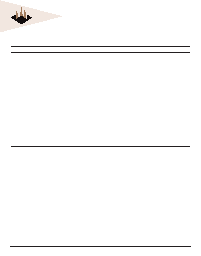
DDR2 ICC SPECIFICATIONS AND CONDITIONS
DDR2 SDRAM components only
VCC = +1.8V ± 0.1V
Parameter
Symbol Condition
806
665
534
403
Units
Operating one device
bank active-precharge
current;
ICC0
tCK = tCK (ICC), tRC = tRC (ICC), tRAS = tRAS MIN (ICC); CKE is HIGH, CS# is
HIGH between valid commands; Address bus inputs are SWITCHING;
Data bus inputs are SWITCHING.
TBD
800
640
mA
Operating one device
bank active-read-
precharge current;
ICC1
IOUT = 0mA; BL = 4, CL = CL(ICC), AL = 0; tCK = tCK (ICC), tRC = tRC (ICC),
tRAS = tRAS MIN (ICC), tRCD = tRCD (ICC); CKE is HIGH, CS# is HIGH
between valid commands; Address bus inputs are SWITCHING; Data
pattern is same as ICC4W.
TBD
1,160
760
mA
Precharge power-down
current;
ICC2P
All device banks idle; tCK = tCK (ICC); CKE is LOW; Other control and
address bus inputs are STABLE; Data bus inputs are FLOATING.
TBD
56
40
mA
Precharge quiet
standby current;
ICC2Q
All device banks idle; tCK = tCK (ICC); CKE is HIGH, CS# is HIGH; Other
control and address bus inputs are STABLE; Data bus inputs are
FLOATING.
TBD
480
328
280
mA
Precharge standby
current;
ICC2N
All device banks idle; tCK = tCK (ICC); CKE is HIGH, CS# is HIGH; Other
control and address bus inputs are SWITCHING; Data bus inputs are
SWITCHING.
TBD
520
360
280
mA
Active power-down
current;
ICC3P
All device banks open; tCK = tCK (ICC); CKE is LOW;
Other control and address bus inputs are STABLE;
Data bus inputs are FLOATING.
Fast PDN Exit
MR[12] = 0
TBD
320
240
200
mA
Slow PDN Exit
MR[12] = 1
TBD
80
mA
Active standby current;
ICC3N
All device banks open; tCK = tCK(ICC), tRAS = tRAS MAX (ICC), tRP = tRP(ICC);
CKE is HIGH, CS# is HIGH between valid commands; Other control and
address bus inputs are SWITCHING; Data bus inputs are SWITCHING.
TBD
560
400
320
mA
Operating burst write
current;
ICC4W
All device banks open, Continuous burst writes; BL = 4, CL = CL (ICC),
AL = 0; tCK = tCK (ICC), tRAS = tRAS MAX (ICC), tRP = tRP (ICC); CKE is
HIGH, CS# is HIGH between valid commands; Address bus inputs are
SWITCHING; Data bus inputs are SWITCHING.
TBD
1,440
1,040
960
mA
Operating burst read
current;
ICC4R
All device banks open, Continuous burst reads, IOUT = 0mA; BL = 4, CL
= CL (ICC), AL = 0; tCK = tCK (ICC), tRAS = tRAS MAX (ICC), tRP = tRP (ICC);
CKE is HIGH, CS# is HIGH between valid commands; Address bus
inputs are SWITCHING; Data bus inputs are SWITCHING.
TBD
1,640
1,160
1,080
mA
Burst refresh current;
ICC5
tCK = tCK (ICC); Refresh command at every tRFC (ICC) interval; CKE
is HIGH, CS# is HIGH between valid commands; Other control and
address bus inputs are SWITCHING; Data bus inputs are SWITCHING.
TBD
2,160
2,000
1,920
mA
Self refresh current;
ICC6
CK and CK# at 0V; CKE ≤ 0.2V; Other control and address bus inputs
are FLOATING; Data bus inputs are FLOATING.
TBD
56
40
mA
Operating device bank
interleave read current;
ICC7
All device banks interleaving reads, IOUT= 0mA; BL = 4, CL = CL (ICC),
AL = tRCD (ICC)-1 x tCK (ICC); tCK = tCK (ICC), tRC = tRC(ICC), tRRD = tRRD(ICC),
tRCD = tRCD(ICC); CKE is HIGH, CS# is HIGH between valid commands;
Address bus inputs are STABLE during DESELECTs; Data bus inputs
are SWITCHING
TBD
2,720
2,360
mA
Note:
ICC specication is based on
MICRON components. Other DRAM manufacturers specication may be different.
相關PDF資料 |
PDF描述 |
|---|---|
| W3HG128M64EEU806D4SG | 128M X 64 DDR DRAM MODULE, 0.45 ns, ZMA200 |
| W3HG128M64EEU665D4ISG | 128M X 64 DDR DRAM MODULE, 0.45 ns, ZMA200 |
| W3HG128M72AEF665F1SAG | DDR DRAM MODULE, DMA240 |
| W3HG128M72AEF534F1GBG | DDR DRAM MODULE, DMA240 |
| W3HG128M72AEF665F1GCG | DDR DRAM MODULE, DMA240 |
相關代理商/技術參數(shù) |
參數(shù)描述 |
|---|---|
| W3HG128M64EEU534D4XXG | 制造商:WEDC 制造商全稱:White Electronic Designs Corporation 功能描述:1GB - 128Mx64 DDR2 SDRAM UNBUFFERED, SO-DIMM |
| W3HG128M64EEU665D4XXG | 制造商:WEDC 制造商全稱:White Electronic Designs Corporation 功能描述:1GB - 128Mx64 DDR2 SDRAM UNBUFFERED, SO-DIMM |
| W3HG128M64EEU806D4XXG | 制造商:WEDC 制造商全稱:White Electronic Designs Corporation 功能描述:1GB - 128Mx64 DDR2 SDRAM UNBUFFERED, SO-DIMM |
| W3HG128M64EEU-D4 | 制造商:WEDC 制造商全稱:White Electronic Designs Corporation 功能描述:1GB - 128Mx64 DDR2 SDRAM UNBUFFERED, SO-DIMM |
| W3HG128M64EEUXXXD4IMG | 制造商:WEDC 制造商全稱:White Electronic Designs Corporation 功能描述:1GB - 128Mx64 DDR2 SDRAM UNBUFFERED, SO-DIMM |
發(fā)布緊急采購,3分鐘左右您將得到回復。