- 您現(xiàn)在的位置:買賣IC網(wǎng) > PDF目錄68457 > W3HG2128M72ACER806AD6IMG (WHITE ELECTRONIC DESIGNS CORP) 256M X 72 DDR DRAM MODULE, DMA240 PDF資料下載
參數(shù)資料
| 型號: | W3HG2128M72ACER806AD6IMG |
| 廠商: | WHITE ELECTRONIC DESIGNS CORP |
| 元件分類: | DRAM |
| 英文描述: | 256M X 72 DDR DRAM MODULE, DMA240 |
| 封裝: | ROHS COMPLIANT, DIMM-240 |
| 文件頁數(shù): | 9/13頁 |
| 文件大小: | 305K |
| 代理商: | W3HG2128M72ACER806AD6IMG |
W3HG2128M72ACER-xAD6
PRELIMINARY
5
White Electronic Designs Corporation (602) 437-1520 www.whiteedc.com
White Electronic Designs
May 2007
Rev. 9
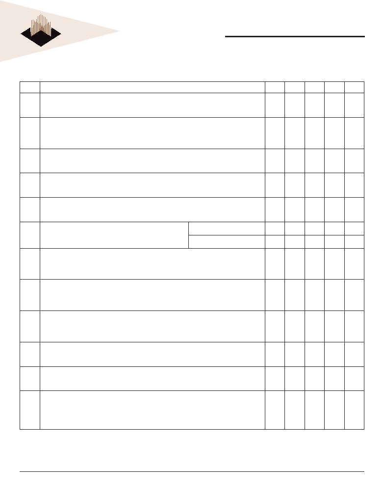
DDR2 ICC SPECIFICATIONS AND CONDITIONS
Includes DDR2 SDRAM components only
Symbol Proposed Conditions
806
665
534
403
Units
ICC0
Operating one bank active-precharge current;
tCK = tCK(ICC), tRC = tRC(ICC), tRAS = tRASmin(ICC); CKE is HIGH, CS# is HIGH between valid commands;
Address bus inputs are SWITCHING; Data bus inputs are SWITCHING
TBD
1,720
1,530
mA
ICC1
Operating one bank active-read-precharge current;
IOUT = 0mA; BL = 4, CL = CL(ICC), AL = 0; tCK = tCK(ICC), tRC = tRC (ICC), tRAS = tRASmin(ICC), tRCD =
tRCD(ICC); CKE is HIGH, CS# is HIGH between valid commands; Address bus inputs are SWITCHING;
Data pattern is same as ICC4W
TBD
1,980
1,800
1,710
mA
ICC2P
Precharge power-down current;
All banks idle; tCK = tCK(ICC); CKE is LOW; Other control and address bus inputs are STABLE; Data
bus inputs are FLOATING
TBD
180
mA
ICC2Q
Precharge quiet standby current;
All banks idle; tCK = tCK(ICC); CKE is HIGH, CS# is HIGH; Other control and address bus inputs are
STABLE; Data bus inputs are FLOATING
TBD
1,800
1,440
1,260
mA
ICC2N
Precharge standby current;
All banks idle; tCK = tCK(ICC); CKE is HIGH, CS# is HIGH; Other control and address bus inputs are
SWITCHING; Data bus inputs are SWITCHING
TBD
1,980
1,620
1,440
mA
ICC3P
Active power-down current;
All banks open; tCK = tCK(ICC); CKE is LOW; Other control and
address bus inputs are STABLE; Data bus inputs are FLOATING
Fast PDN Exit MRS(12) = 0
TBD
1,260
1,080
900
mA
Slow PDN Exit MRS(12) = 1
TBD
360
mA
ICC3N
Active standby current;
All banks open; tCK = tCK(ICC), tRAS = tRASmax(ICC), tRP = tRP(ICC); CKE is HIGH, CS# is HIGH between
valid commands; Other control and address bus inputs are SWITCHING; Data bus inputs are
SWITCHING
TBD
2,340
1,980
1,620
mA
ICC4W
Operating burst write current;
All banks open, Continuous burst writes; BL = 4, CL = CL(ICC), AL = 0; tCK = tCK(ICC), tRAS =
tRASmax(ICC), tRP = tRP(ICC); CKE is HIGH, CS# is HIGH between valid commands; Address bus inputs
are SWITCHING; Data bus inputs are SWITCHING
TBD
2,880
2,430
2,070
mA
ICC4R
Operating burst read current;
All banks open, Continuous burst reads, IOUT = 0mA; BL = 4, CL = CL(ICC), AL = 0; tCK = tCK(ICC), tRAS =
tRASmax(ICC), tRP = tRP(ICC); CKE is HIGH, CS# is HIGH between valid commands; Address bus inputs
are SWITCHING; Data pattern is same as ICC4W
TBD
3,240
2,700
2,160
mA
ICC5B
Burst auto refresh current;
tCK = tCK(ICC); Refresh command at every tRFC(ICC) interval; CKE is HIGH, CS# is HIGH between valid
commands; Other control and address bus inputs are SWITCHING; Data bus inputs are SWITCHING
TBD
7,560
7,200
6,840
mA
ICC6
Self refresh current;
CK and CK# at 0V; CKE 0.2V; Other control and address bus inputs
are FLOATING; Data bus inputs are FLOATING
TBD
180
mA
ICC7
Operating bank interleave read current;
All bank interleaving reads, IOUT = 0mA; BL = 4, CL = CL(ICC), AL = tRCD(ICC)-1*tCK(ICC); tCK = tCK(ICC),
tRC = tRC(ICC), tRRD = tRRD(ICC), tRCD = 1*tCK(ICC); CKE is HIGH, CS# is HIGH between valid commands;
Address bus inputs are STABLE during DESELECTs; Data pattern is same as ICC4R; Refer to the
following page for detailed timing conditions
TBD
5,130
4,770
4,230
mA
NOTE: ICC specs are based on
MICRON components. Other DRAM manufacturers parameters may be different.
相關(guān)PDF資料 |
PDF描述 |
|---|---|
| W3HG2128M72ACER534AD6IMG | 256M X 72 DDR DRAM MODULE, 0.5 ns, DMA240 |
| W3HG2128M72ACER806AD6IMG | 256M X 72 DDR DRAM MODULE, DMA240 |
| W3HG2128M72ACER806AD6SG | 256M X 72 DDR DRAM MODULE, DMA240 |
| W3HG2128M72ACER665AD6SG | 256M X 72 DDR DRAM MODULE, 0.45 ns, DMA240 |
| W3HG2128M72ACER534AD6SG | 256M X 72 DDR DRAM MODULE, 0.5 ns, DMA240 |
相關(guān)代理商/技術(shù)參數(shù) |
參數(shù)描述 |
|---|---|
| W3HG2128M72ACER806AD6XG | 制造商:WEDC 制造商全稱:White Electronic Designs Corporation 功能描述:2GB - 2x128Mx72 DDR2 SDRAM REGISTERED, w/PLL, VLP |
| W3HG2128M72ACER-AD6 | 制造商:WEDC 制造商全稱:White Electronic Designs Corporation 功能描述:2GB - 2x128Mx72 DDR2 SDRAM REGISTERED, w/PLL, VLP |
| W3HG2128M72ACERXXXAD6MG | 制造商:WEDC 制造商全稱:White Electronic Designs Corporation 功能描述:2GB - 2x128Mx72 DDR2 SDRAM REGISTERED, w/PLL, VLP |
| W3HG2128M72ACERXXXAD6SG | 制造商:WEDC 制造商全稱:White Electronic Designs Corporation 功能描述:2GB - 2x128Mx72 DDR2 SDRAM REGISTERED, w/PLL, VLP |
| W3HG264M72EER403AD7XG | 制造商:WEDC 制造商全稱:White Electronic Designs Corporation 功能描述:1GB - 2x64Mx72 DDR2 SDRAM REGISTERED, w/PLL, VLP Mini-DIMM |
發(fā)布緊急采購,3分鐘左右您將得到回復(fù)。