- 您現(xiàn)在的位置:買賣IC網(wǎng) > PDF目錄361786 > W53322 PDF資料下載
參數(shù)資料
| 型號(hào): | W53322 |
| 文件頁數(shù): | 5/8頁 |
| 文件大?。?/td> | 94K |
| 代理商: | W53322 |
W53322/ W53342
Publication Release Date: March 1999
- 5 - Revision A2
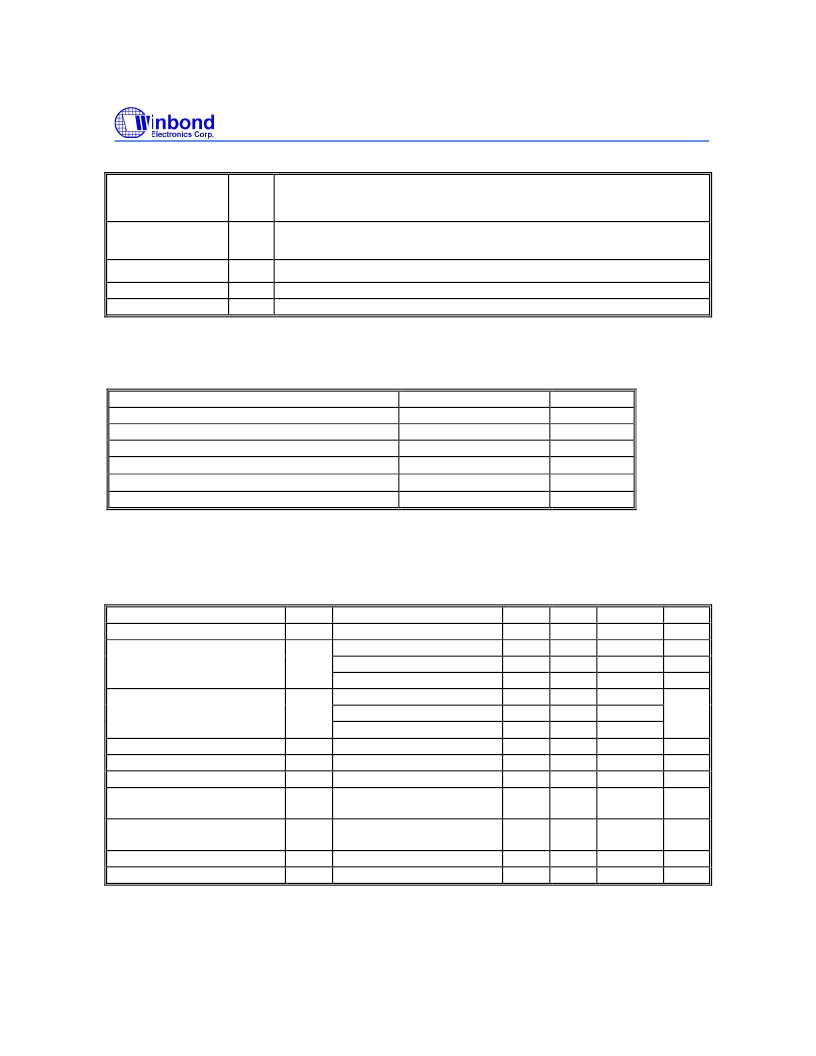
V2 ~ V5
O
LCD COM/SEG output driving voltage. If internal shunt resistor is
disabled, external resistors need to be supplied to V2, V3, V4, V5 . A
capacitor is suggested for stable LCD voltage level.
External variable resistor connects between VDD3 and V6 to adjust
LCD maximun voltage level.
V6
I
VDD
I
Microcontroller Positive power supply (+).
Negative power supply (-).
Negative power supply (-).
VSS1
VSS2
I
I
ABSOLUTE MAXIMUM RATINGS
PARAMETER
Supply Voltage to Ground Potential
Applied Input/Output Voltage
Power Dissipation
Ambient Operating Temperature
Storage Temperature
VDD3 Input Voltage
Note: Exposure to conditions beyond those listed under Absolute Maximum Ratings may adversely
affect the life and reliability of the device.
RATING
-0.3 to +7.0
-0.3 to +7.0
120
0 to +70
-55 to +150
12
UNIT
V
V
mW
°
C
°
C
V
DC CHARACTERISTICS
(VDD
VSS = 3.0V, Fm =1 MHz, Fs = 32.768 KHz, TA = 25
°
C, LCD on; unless otherwise specified)
PARAMETER
SYM.
CONDITIONS
Op. Voltage
V
DD
Op. Current
I
OP1
Dual clock with crystal
(No Load)
Dual clock with RC type
Single Clock
Halt Mode Current
Iop2
Dual clock with crystal
(No Load, LCD OFF)
Dual clock with RC type
Single clock
Stop Mode Current
Iop3
LCD OFF
Input Low Voltage
V
IL
-
Input High Voltage
V
IH
-
Port RA, RB Output Low
Voltage
Port RA, RB Output High
Voltage
Port RE Sink Current
I
EL
VOL = 0.4V
Port RE Source Current
I
EH
VOH = 2.4V
MIN.
2.4
-
TYP.
MAX.
5.5
300
300
100
150
150
10
1
0.3*VDD
1
0.4
UNIT
V
uA
uA
uA
uA
250
250
60
120
120
6
uA
V
VDD
V
VSS
0.7
-
-
-
-
V
ABL
IOL = 2.0 mA
V
ABH
IOH = -2.0 mA
2.4
-
-
V
2
-2
-
-
-
-
mA
mA
相關(guān)PDF資料 |
PDF描述 |
|---|---|
| W53342 | |
| W5360120A | |
| W5360120P | |
| W5360120T | |
| W536020A | ViewTalkTM Family |
相關(guān)代理商/技術(shù)參數(shù) |
參數(shù)描述 |
|---|---|
| W533273 | 制造商:COOPER INDUSTRIES 功能描述:Block Clutch Mold #675 Loc K5 UL |
| W53342 | 制造商:未知廠家 制造商全稱:未知廠家 功能描述: |
| W5339 | 制造商:Tamura Corporation of America 功能描述: |
| W53481132SARC | 制造商:Winslow Adaptics Ltd 功能描述:32 way 1 row through board socket,1.27mm |
| W53482120SARC | 制造商:Winslow Adaptics Ltd 功能描述:20 way 2 row through board socket,1.27mm |
發(fā)布緊急采購(gòu),3分鐘左右您將得到回復(fù)。