- 您現(xiàn)在的位置:買賣IC網(wǎng) > PDF目錄361787 > W541L250 4-Bit Microcontroller PDF資料下載
參數(shù)資料
| 型號: | W541L250 |
| 英文描述: | 4-Bit Microcontroller |
| 中文描述: | 4位微控制器 |
| 文件頁數(shù): | 5/7頁 |
| 文件大小: | 49K |
| 代理商: | W541L250 |
W541C250
Publication Release Date: Feb 2002
- 5 -
Revision A2
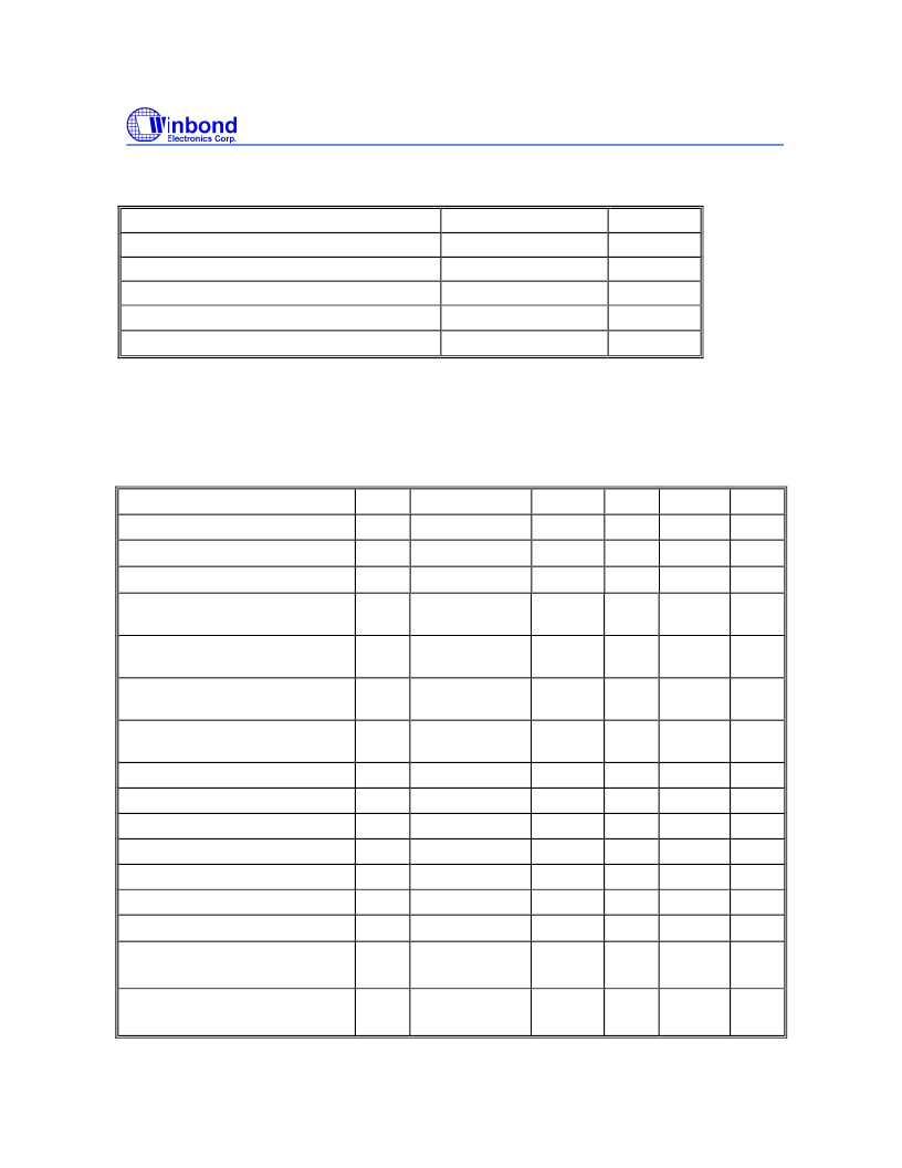
ABSOLUTE MAXIMUM RATINGS
PARAMETER
RATING
-0.3 to +7.0
-0.3 to +7.0
120
0 to +70
UNIT
V
V
mW
°
C
°
C
Supply Voltage to Ground Potential
Applied Input/Output Voltage
Power Dissipation
Ambient Operating Temperature
Storage Temperature
-55 to +150
Note: Exposure to conditions beyond those listed under Absolute Maximum Ratings may adversely affect the life and reliability
of the device.
DC CHARACTERISTICS
(V
DD
V
SS
= 3.0V, F
OSC
. = 32.768 KHz, T
A
= 25
°
C; unless otherwise specified)
PARAMETER
SYM.
CONDITIONS
MIN.
TYP.
MAX.
UNIT
Op. Voltage
V
DD
-
2.4
-
5.5
V
Op. Current (Crystal type)
I
OP1
No load (Ext-V)
-
-
20
μ
A
Op. Current (RC type)
I
OP2
No load (Ext-V)
-
-
65
μ
A
Hold Current (Crystal type)
I
HM1
Hold mode
No load (Ext-V)
-
-
6
μ
A
Hold Current (RC type)
I
HM2
Hold mode
No load (Ext-V)
-
-
40
μ
A
Stop Current (Crystal type)
I
SM1
Stop mode
No load (Ext-V)
-
0.1
2
μ
A
Stop Current (RC type)
I
SM2
Stop mode
No load (Ext-V)
-
0.1
2
μ
A
Input Low Voltage
V
IL
-
V
SS
-
0.3 V
DD
V
Input High Voltage
V
IH
-
0.7 V
DD
-
V
DD
V
MFP Output Low Voltage
V
ML
I
OL
= 3.5 mA
-
-
0.4
V
MFP Output High Voltage
V
MH
I
OH
= -3.5 mA
2.4
-
-
V
Port RA, RB Output Low Voltage
V
ABL
I
OL
= 2.0 mA
-
-
0.4
V
Port RA, RB Output high Voltage
V
ABH
I
OH
= -2.0 mA
2.4
-
-
V
LCD Supply Current
I
LCD
All Seg. On
-
-
10
μ
A
SEG0
SEG23 Sink Current
(work as LCD output pins)
I
OL
V
OL
= 0.4V
V
LCD
= 0.0V
0.4
-
-
μ
A
SEG0
SEG23 Drive Current
(work as LCD output pins)
I
OH
V
OH
= 2.4V
V
LCD
= 3.0V
-0.3
-
-
μ
A
相關(guān)PDF資料 |
PDF描述 |
|---|---|
| W551C002 | Interactive Toy Family |
| W551C005 | Interactive Toy Family |
| W551C010 | Interactive Toy Family |
| W551C020 | Interactive Toy Family |
| W551C040 | Interactive Toy Family |
相關(guān)代理商/技術(shù)參數(shù) |
參數(shù)描述 |
|---|---|
| W541L260 | 制造商:WINBOND 制造商全稱:Winbond 功能描述:4-BIT MICROCONTROLLER |
| W54318A-0402TSG WAF | 制造商:SMSC 功能描述: |
| W5437 | 制造商:Thomas & Betts 功能描述:WRENCH 制造商:Belden Inc 功能描述: |
| W54NK30Z | 制造商:STMicroelectronics 功能描述: |
| W54-XA1A4A10-15 | 制造商:TE Connectivity 功能描述: |
發(fā)布緊急采購,3分鐘左右您將得到回復(fù)。