- 您現(xiàn)在的位置:買賣IC網(wǎng) > PDF目錄361788 > W566B025 Microcontroller PDF資料下載
參數(shù)資料
| 型號: | W566B025 |
| 英文描述: | Microcontroller |
| 中文描述: | 微控制器 |
| 文件頁數(shù): | 5/18頁 |
| 文件大?。?/td> | 130K |
| 代理商: | W566B025 |
W566BXXX
Publication Release Date: April 24, 2002
- 5 -
Revision A1
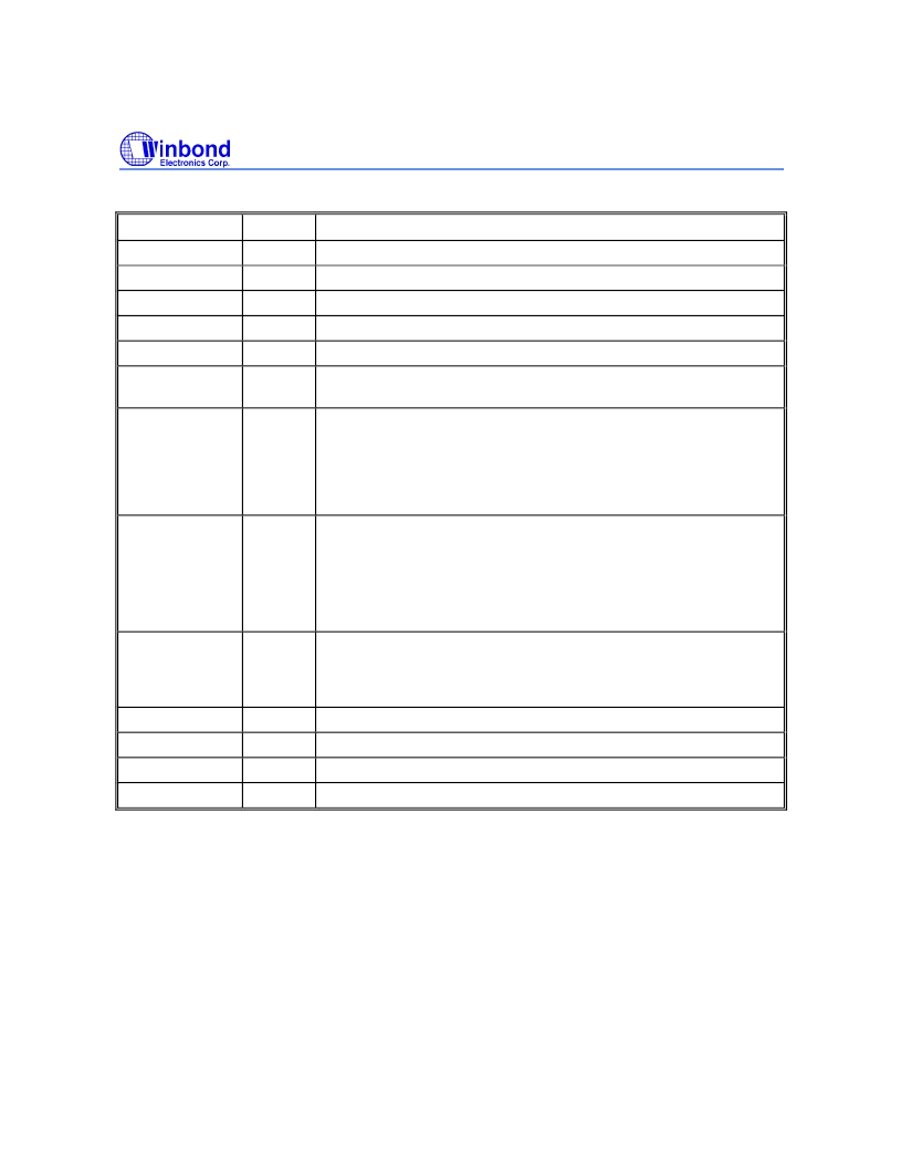
3. PIN DESCRIPTION
PIN NAME
I/O
FUNCTION
RESETB
In
IC reset input.
XIN
In
Sub-clock oscillation input. Only RC type is allowed.
XOUT
Out
Sub-clock oscillation output.
OSCI
In
Main-clock oscillation input.
OSCO
Out
Main-clock oscillation output.
OSCSEL
In
Pin selection of main-clock type. When OSCSEL is logic 1, Ring type
is used. When OSCSEL is logic 0, crystal type is used.
IP0[7:4]
(Expect
W566B100,
W566B120,
W566B150, &
W566B170)
In
General input port with pull-high selection. Each input pin can be
programmed to generate interrupt request and used to release IC
from HOLD/STOP mode.
IP0.6 can be used as the external clock source of the general timer
TimerG.
BP0[7:0]
I/O
General input/output pins. When used as output pin, it can be open–
drain or CMOS type and it can sink 8mA for high-current application.
When used as input pin, there may have a pull-high option and
generate interrupt request to release IC from HOLD/STOP mode.
When BP0[7] is used as output pin, it can be the IR transmission
carrier for firmware IR application.
BP1[7:0]
I/O
General input/output pins. When used as output pin, it can be open–
drain or CMOS type. When used as input pin, there may have a pull-
high option and generate interrupt request to release IC from
HOLD/STOP mode.
DAC
Out
Current type speaker output.
TEST
In
Test input. Do not connect during normal operation.
V
DD
Power
Positive power supply.
V
SS
Power
Negative power supply.
相關(guān)PDF資料 |
PDF描述 |
|---|---|
| W566B030 | BandDirectorTM Family |
| W566B040 | Microcontroller |
| W566B060 | BandDirectorTM Family |
| W566C | BandDirectorTM Family |
| W58101 | Speech Synthesizer |
相關(guān)代理商/技術(shù)參數(shù) |
參數(shù)描述 |
|---|---|
| W5675C3K1 | 制造商:TAN 功能描述:WS656X075 |
| W56-75C3K1 | 制造商:TAN 功能描述:WS656X075 |
| W5675C3M1 | 制造商:TAN 功能描述:WS656X075 TANSITOR S9K4A |
| W567B080 | 制造商:未知廠家 制造商全稱:未知廠家 功能描述:BandDirectorTM Family |
| W567B100 | 制造商:未知廠家 制造商全稱:未知廠家 功能描述:BandDirectorTM Family |
發(fā)布緊急采購,3分鐘左右您將得到回復(fù)。