- 您現(xiàn)在的位置:買(mǎi)賣(mài)IC網(wǎng) > PDF目錄361793 > W78M32V70BM 8Mx32 Flash 3.3V Page Mode Simultaneous Read/Write Operation Multi-Chip Package PDF資料下載
參數(shù)資料
| 型號(hào): | W78M32V70BM |
| 英文描述: | 8Mx32 Flash 3.3V Page Mode Simultaneous Read/Write Operation Multi-Chip Package |
| 中文描述: | 8Mx32閃光3.3V的頁(yè)面模式同步讀/寫(xiě)操作多芯片封裝 |
| 文件頁(yè)數(shù): | 34/54頁(yè) |
| 文件大?。?/td> | 756K |
| 代理商: | W78M32V70BM |
第1頁(yè)第2頁(yè)第3頁(yè)第4頁(yè)第5頁(yè)第6頁(yè)第7頁(yè)第8頁(yè)第9頁(yè)第10頁(yè)第11頁(yè)第12頁(yè)第13頁(yè)第14頁(yè)第15頁(yè)第16頁(yè)第17頁(yè)第18頁(yè)第19頁(yè)第20頁(yè)第21頁(yè)第22頁(yè)第23頁(yè)第24頁(yè)第25頁(yè)第26頁(yè)第27頁(yè)第28頁(yè)第29頁(yè)第30頁(yè)第31頁(yè)第32頁(yè)第33頁(yè)當(dāng)前第34頁(yè)第35頁(yè)第36頁(yè)第37頁(yè)第38頁(yè)第39頁(yè)第40頁(yè)第41頁(yè)第42頁(yè)第43頁(yè)第44頁(yè)第45頁(yè)第46頁(yè)第47頁(yè)第48頁(yè)第49頁(yè)第50頁(yè)第51頁(yè)第52頁(yè)第53頁(yè)第54頁(yè)
34
White Electronic Designs Corporation (602) 437-1520 www.wedc.com
White Electronic Designs
W78M32V-XBX
April 2006
Rev. 3
White Electronic Designs Corp. reserves the right to change products or specifications without notice.
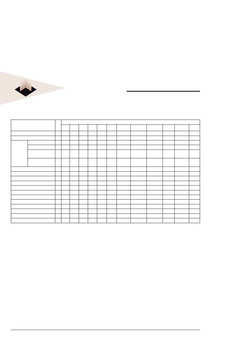
COMMAND DEFINITIONS TABLES
TABLE 13. MEMORY ARRAY COMMAND DEFINITIONS
Command (Notes)
C
Bus Cycles (Notes 1-4)
Addr
Addr
Data
Addr
Data
Addr
Data
Data
Addr
Data
Addr
Data
Read (5)
Reset (6)
Autoselect
(Note 7)
1
1
4
6
4
RA
XXX
555
555
555
RD
F0
AA
AA
AA
Manufacturer ID
Device ID (10)
SecSi Sector
Factory Protect (8)
Sector Group
Protect Verify (9)
2AA
2AA
2AA
55
55
55
555
555
555
90
90
90
(BA)X00
(BA)X0
X03
04
7E
(BA)X0E
20
(BA)X0F
00
(see note
8)
XX00/
XX01
PD
AA
AA
4
555
AAA
2AA
55
555
90
(SA)X02
Program
Chip Erase
Sector Erase
Program/Erase Suspend (11)
Program/Erase Resume (12)
CFI Query (13)
Accelerated Program (15)
Unlock Bypass Entry (15)
Unlock Bypass Program (15)
Unlock Bypass Erase (15)
Unlock Bypass CFI (13, 15)
Unlock Bypass Reset (15)
Legend:
BA = Address of bank switching to autoselect mode, bypass mode, or erase
operation. Determined by A22:A20, see Tables
4
and for more detail.
PA = Program Address (A22:A0). Addresses latch on falling edge of
WE# or CS# pulse, whichever happens later.
PD = Program Data (DQ15:DQ0) for each chip written to location PA. Data latches
on rising edge of WE# or CS# pulse, whichever happens first.
4
6
6
1
1
1
2
3
2
2
1
2
555
555
555
BA
BA
55
XX
555
XX
XX
XX
XXX
AA
AA
AA
B0
30
98
A0
AA
A0
80
98
90
2AA
2AA
2AA
55
55
55
555
555
555
A0
80
80
PA
555
555
2AA
2AA
55
55
555
SA
10
30
PA
2AA
PA
XX
PD
55
PD
10
555
20
XXX
00
RA = Read Address (A22:A0).
RD = Read Data (DQ15:DQ0) from location RA.
SA = Sector Address (A22:A12) for verifying (in autoselect mode) or erasing.
WD = Write Data. See “Configuration Register” definition for specific write data. Data
latched on rising edge of WE#.
X = Don’t care
Notes:
1. See
Table 1
for description of bus operations.
2. All values are in hexadecimal.
3. Shaded cells in table denote read cycles. All other cycles are write operations.
4. During unlock and command cycles, when lower address bits are 555 or 2AAh as
shown in table, address bits higher than A11 (except where BA is required) and data
bits higher than DQ7 are don’t cares.
5. No unlock or command cycles required when bank is reading array data.
6. The Reset command is required to return to reading array (or to erase-suspend-read
mode if previously in Erase Suspend) when bank is in autoselect mode, or if DQ5
goes high (while bank is providing status information).
7. Fourth cycle of autoselect command sequence is a read cycle. System must provide
bank address to obtain manufacturer ID or device ID information. See
Autoselect
Command Sequence
section for more information.
8. The data is C0h for factory and customer locked and 80h for factory locked.
9. The data is 00h for an unprotected sector group and 01h for a protected sector
group.
10. Device ID must be read across cycles 4, 5, and 6.
11. System may read and program in non-erasing sectors, or enter autoselect
mode, when in Program/Erase Suspend mode. Program/Erase Suspend
command is valid only during a sector erase operation, and requires bank
address.
12. Program/Erase Resume command is valid only during Erase
Suspend mode, and requires bank address.
13. Command is valid when device is ready to read array data or when device is In
autoselect mode.
14. WP#/ACC must be at V
ID
during the entire operation of command.
15. Unlock Bypass Entry command is required prior to any Unlock Bypass
operation. Unlock Bypass Reset command is required to return to the reading
array.
相關(guān)PDF資料 |
PDF描述 |
|---|---|
| W78M32V90BC | 8Mx32 Flash 3.3V Page Mode Simultaneous Read/Write Operation Multi-Chip Package |
| W78M32V90BI | 8Mx32 Flash 3.3V Page Mode Simultaneous Read/Write Operation Multi-Chip Package |
| W78M32V90BM | 8Mx32 Flash 3.3V Page Mode Simultaneous Read/Write Operation Multi-Chip Package |
| W78M32V-XBX | 8Mx32 Flash 3.3V Page Mode Simultaneous Read/Write Operation Multi-Chip Package |
| W78M64V-XSBX | Flash MCP |
相關(guān)代理商/技術(shù)參數(shù) |
參數(shù)描述 |
|---|---|
| W78M32V90BC | 制造商:WEDC 制造商全稱(chēng):White Electronic Designs Corporation 功能描述:8Mx32 Flash 3.3V Page Mode Simultaneous Read/Write Operation Multi-Chip Package |
| W78M32V90BI | 制造商:WEDC 制造商全稱(chēng):White Electronic Designs Corporation 功能描述:8Mx32 Flash 3.3V Page Mode Simultaneous Read/Write Operation Multi-Chip Package |
| W78M32V90BM | 制造商:WEDC 制造商全稱(chēng):White Electronic Designs Corporation 功能描述:8Mx32 Flash 3.3V Page Mode Simultaneous Read/Write Operation Multi-Chip Package |
| W78M32VP110BM | 制造商:Microsemi Corporation 功能描述:W78M32VP110BM - Bulk |
| W78M32VP-110BM | 制造商:White Electronic Designs 功能描述:Flash Module Parallel 256Mbit |
發(fā)布緊急采購(gòu),3分鐘左右您將得到回復(fù)。