- 您現(xiàn)在的位置:買賣IC網(wǎng) > PDF目錄204017 > WED48S8030E10SI (MICROSEMI CORP-PMG MICROELECTRONICS) 8M X 8 SYNCHRONOUS DRAM, 6 ns, PDSO54 PDF資料下載
參數(shù)資料
| 型號: | WED48S8030E10SI |
| 廠商: | MICROSEMI CORP-PMG MICROELECTRONICS |
| 元件分類: | DRAM |
| 英文描述: | 8M X 8 SYNCHRONOUS DRAM, 6 ns, PDSO54 |
| 封裝: | TSOP2-54 |
| 文件頁數(shù): | 12/26頁 |
| 文件大?。?/td> | 920K |
| 代理商: | WED48S8030E10SI |
第1頁第2頁第3頁第4頁第5頁第6頁第7頁第8頁第9頁第10頁第11頁當(dāng)前第12頁第13頁第14頁第15頁第16頁第17頁第18頁第19頁第20頁第21頁第22頁第23頁第24頁第25頁第26頁
WED48S8030E
2
White Electronic Designs Corporation (602) 437-1520 www.whiteedc.com
White Electronic Designs
White Electronic Designs Corp. reserves the right to change products or specications without notice.
February, 2002
Rev. 2
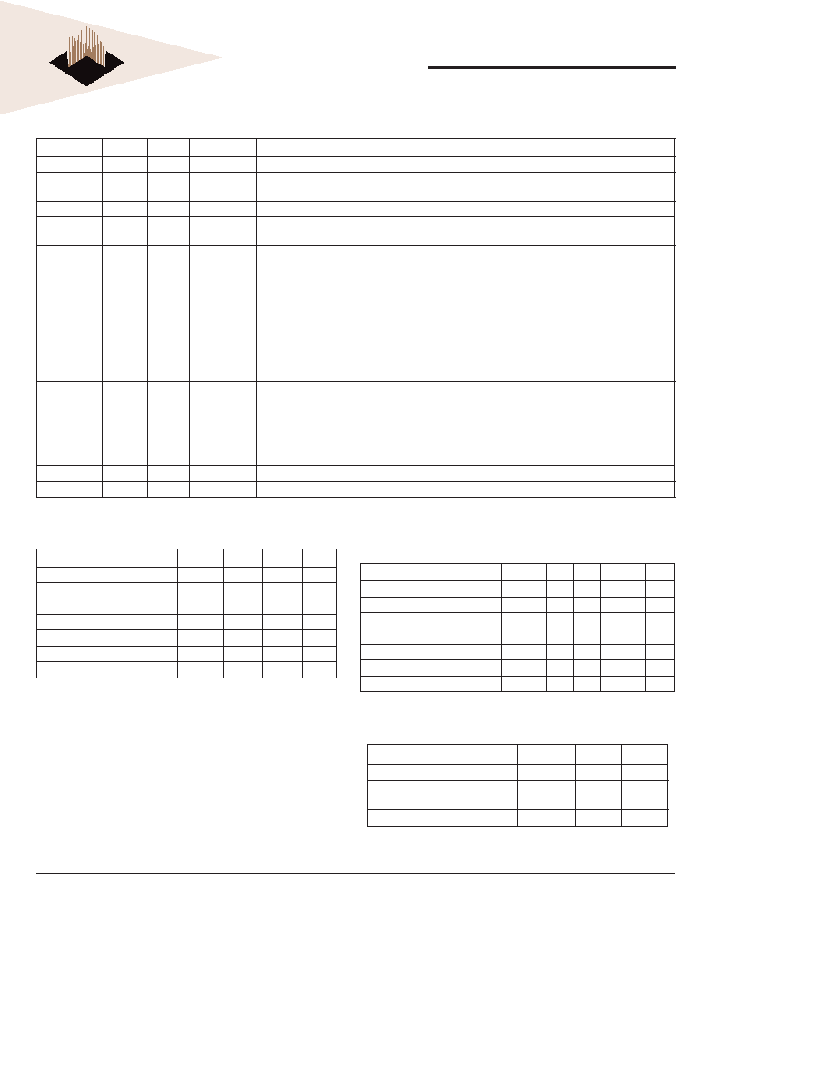
INPUT/OUTPUT FUNCTIONAL DESCRIPTION
Symbol
Type
Signal
Polarity
Function
CK
Input
Pulse
Positive Edge The system clock input. All of the SDRAM inputs are sampled on the rising edge of the clock.
CKE
Input
Level
Active High
Activates the CK signal when high and deactivates the CK signal when low. By deactivating the clock,
CKE low initiates the Power Down mode, Suspend mode, or the Self Refresh mode.
CE#
Input
Pulse
Active Low
CE# disable or enable device operation by masking or enabling all inputs except CK, CKE and DQM.
RAS#, CAS#
WE#
Input
Pulse
Active Low
When sampled at the positive rising edge of the clock, CAS#, RAS#, and WE# dene the operation to
be executed by the SDRAM.
BA0,BA1
Input
Level
—
Selects which SDRAM bank is to be active.
A0-11,
A10/AP
Input
Level
—
During a Bank Activate command cycle, A0-11 denes the row address (RA0-11) when sampled at the
rising clock edge. During a Read or Write command cycle, A0-7 denes the column address (CA0-7)
when sampled at the rising clock edge. In addition to the row address, A10/AP is used to invoke
Autoprecharge operation at the end of the Burst Read or Write cycle. If A10/AP is high, autoprecharge
is selected and BA0, BA1 denes the bank to be precharged . If A10/AP is low, autoprecharge is
disabled.
During a Precharge command cycle, A10/AP is used in conjunction with BA0, BA1 to control which
bank(s) to precharge. If A10/AP is high, all banks will be precharged regardless of the state of BA0,
BA1. If A10/AP is low, then BA0, BA1 is used to dene which bank to precharge.
DQ0-15
Input/
Output
Level
—
Data Input/Output are multiplexed on the same pins
DQM
Input
Pulse
Mask
Active High
The Data Input/Output mask places the DQ buffers in a high impedance state when sampled high.
In Read mode, DQM has a latency of two clock cycles and controls the output buffers like an output
enable. In Write mode, DQM has a latency of zero and operates as a word mask by allowing input data
to be written if it is low but blocks the Write operation if DQM is high.
VCC, VSS
Supply
Power and ground for the input buffers and the core logic.
VCCQ, VSSQ
Supply
Isolated power and ground for the output buffers to improve noise immunity.
Recommended DC Operating Conditions
(Voltage Referenced to: VSS = 0V, TA = 40°C to +85°C)
Absolute Maximum Ratings
Parameter
Symbol Min Typ
Max
Unit
Supply Voltage
VCC
3.0
3.3
3.6
V
Input High Voltage
VIH
2.0
3.0
VCC +0.3
V
Input Low Voltage
VIL
-0.3
—
0.8
V
Output High Voltage (IOH = -2mA)
VOH
2.4
—
V
Output Low Voltage (IOL = 2mA)
VOL
—
0.4
V
Input Leakage Voltage
IIL
-10
—
10
μA
Output Leakage Voltage
IOL
-10
—
10
μA
Capacitance
(TA = 25°C, f = 1MHz, VCC = 3.3V to 3.6V)
Parameter
Symbol
Min
Max
Units
Power Supply Voltage
VCC
-1.0
+4.6
V
Input Voltage
VIN
-1.0
+4.6
V
Output Voltage
VOUT
-1.0
+4.6
V
Operating Temperature
TOPR
-40
+85
°C
Storage Temperature
TSTG
-55
+125
°C
Power Dissipation
PD
—
1.0
W
Short Circuit Output Current
IOS
—50
mA
Stress greater than those listed under "Absolute Maximum Ratings" may cause
permanent damage to the device. This is a stress rating only and functional
operation of the device at these or any other conditions greater than those indicated
in the operational sections of this specication is not implied. Exposure to absolute
maximum rating conditions for extended periods may affect reliability.
Parameter
Symbol
Max
Unit
Input Capacitance
CI14
pF
Input Capacitance (CK, CKE,
RAS#, CAS#, WE#, CE#, DQM)
C124
pF
Input/Output Capacitance (DQ)
COUT
5pF
相關(guān)PDF資料 |
PDF描述 |
|---|---|
| WED7P128CFA7001I25 | 8M X 16 FLASH 3V PROM CARD, 250 ns, UUC50 |
| WED8L24514V15BI | 512K X 24 MULTI DEVICE SRAM MODULE, 15 ns, PBGA119 |
| WED9LAPC2C16P8BC | 4M X 32 SYNCHRONOUS DRAM, PBGA153 |
| WEDPN4M64V-125BC | 4M X 64 SYNCHRONOUS DRAM, 6 ns, PBGA219 |
| WEDPN4M64V-125BI | 4M X 64 SYNCHRONOUS DRAM, 6 ns, PBGA219 |
相關(guān)代理商/技術(shù)參數(shù) |
參數(shù)描述 |
|---|---|
| WED48S8030E8SI | 制造商:WEDC 制造商全稱:White Electronic Designs Corporation 功能描述:2M x 8 Bits x 4 Banks Synchronous DRAM |
| WED7F2324XDNSN | 制造商:未知廠家 制造商全稱:未知廠家 功能描述:Intel/Sharp Flash Modules |
| WED7F2324XDNSN12C | 制造商:WEDC 制造商全稱:White Electronic Designs Corporation 功能描述:4Mx32 / 2x4Mx32 INTEL J3 BASED, FLASH MODULE |
| WED7F2325ZXEBSN12C | 制造商:WEDC 制造商全稱:White Electronic Designs Corporation 功能描述:2, 4, and 8MB, STmicro, 5.0V 4Mb Based, Uniform Sector FLASH Module Family |
| WED7F2325ZXEBSN15C | 制造商:WEDC 制造商全稱:White Electronic Designs Corporation 功能描述:2, 4, and 8MB, STmicro, 5.0V 4Mb Based, Uniform Sector FLASH Module Family |
發(fā)布緊急采購,3分鐘左右您將得到回復(fù)。