- 您現(xiàn)在的位置:買賣IC網(wǎng) > PDF目錄202127 > WED7G097ATA33XDC25 (MICROSEMI CORP-PMG MICROELECTRONICS) 48M X 16 FLASH 3.3V PROM MODULE, DMA144 PDF資料下載
參數(shù)資料
| 型號(hào): | WED7G097ATA33XDC25 |
| 廠商: | MICROSEMI CORP-PMG MICROELECTRONICS |
| 元件分類: | PROM |
| 英文描述: | 48M X 16 FLASH 3.3V PROM MODULE, DMA144 |
| 封裝: | SODIMM-144 |
| 文件頁數(shù): | 3/4頁 |
| 文件大小: | 108K |
| 代理商: | WED7G097ATA33XDC25 |
3
White Electronic Designs Corporation (508) 366-5151 www.whiteedc.com
White Electronic Designs
WED7GxxxATA33
SIGNAL DESCRIPTION
Signal Name
Description
DQ0-DQ7, DQ8-DQ15
Data bus can either be 8-bits or 16-bits wide depending on selection of CE0\ and CE1\
CE0\, CE1\
CE1\ always selects the odd byte of the word. CE0\ accesses the even or odd byte depending on A0 and CE1\. For 8-bit
systems, CE0 is used and for 16-bit systems, both CE0\ and CE1\ are used. Both CE0\ and CE1\ should be decoded by the
logic to determine the memory window.
OE\
This is an output enable strobe generated by the host interface. It is used to read data from the Flash ChipSet in Memory Mode
and to read the CIS and configuration registers
WE\
The write enable pin is driven by the host and used for strobing data to the registers of the Flash ChipSet when the Flash
ChipSet is configured in the memory interface mode. It is also used for writing the configuration registers.
A0-A10
A0-A3 selects the basic registers of the controller to communicate to the module. This requires 16 bytes of host address space.
A0 is optional if CE0\ and CE1\ are combined to enable 16-bit wide register access.
Busy
The Busy signal is driven low when the product is accessing memory. When Busy is high, register access is allowed. After a
data transfer command is issued, this signal is used to signify that the host can transfer data.
RST
When RST is high, the product is placed in a reset mode. This signal is only valid at power on.
BVD1
This signal is driven high since a battery is not used with this product
BVD2This output line is always driven to a high state in Memory Mode since a batery is not required for this product
IOWR
This signal is not used in the memory mode.
IORD
This signal is not used in the memory mode.
REG
This signal is used during Memory Cycles to distinguish between common memory and register memory accesses. High for
common memory, low for attribute memory.
INPACK
This signal is not used in the memory mode.
IO16
Optional test signals not used in the Memory Mapped Mode.
Reserved
Pins are reserved for future expansion and must be left floating.
VCC
Power pins. All VCC pins must be connected.
VSS
Ground pins. All VSS pins must be connected.
NC
No connect. Pin internally not connected.
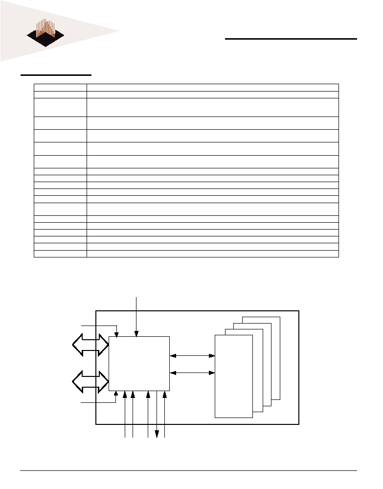
BLOCK DIAGRAM
D0 - D7
CE0
CE1
D8 - D15
A0 - A10
SanDisk
Controller
Data
Control
NAND
Flash
1
2
n
6
WE
OE
RST
BUSY
Control signals used
in other modes (see
pin list)
相關(guān)PDF資料 |
PDF描述 |
|---|---|
| WF128K32N-120H1C5 | 128K X 32 FLASH 5V PROM MODULE, 120 ns, CPGA66 |
| WF128K32N-120H1I5 | 128K X 32 FLASH 5V PROM MODULE, 120 ns, CPGA66 |
| WF512K32-60G2LC5 | 512K X 32 FLASH 5V PROM MODULE, 60 ns, CQFP68 |
| WF512K32-60G2LI5 | 512K X 32 FLASH 5V PROM MODULE, 60 ns, CQFP68 |
| WF512K32-60G2LM5 | 512K X 32 FLASH 5V PROM MODULE, 60 ns, CQFP68 |
相關(guān)代理商/技術(shù)參數(shù) |
參數(shù)描述 |
|---|---|
| WED7G112IDE33ADC25 | 制造商:WEDC 制造商全稱:White Electronic Designs Corporation 功能描述:DimmDrive Solid State IDE Flash Module with Power Failure Protection IDE36 DimmDrive Solid State IDE Flash Module IDE33 |
| WED7G112IDE36ADC25 | 制造商:WEDC 制造商全稱:White Electronic Designs Corporation 功能描述:DimmDrive Solid State IDE Flash Module with Power Failure Protection IDE36 DimmDrive Solid State IDE Flash Module IDE33 |
| WED7G128IDE33ADC25 | 制造商:WEDC 制造商全稱:White Electronic Designs Corporation 功能描述:DimmDrive Solid State IDE Flash Module with Power Failure Protection IDE36 DimmDrive Solid State IDE Flash Module IDE33 |
| WED7G128IDE36ADC25 | 制造商:WEDC 制造商全稱:White Electronic Designs Corporation 功能描述:DimmDrive Solid State IDE Flash Module with Power Failure Protection IDE36 DimmDrive Solid State IDE Flash Module IDE33 |
| WED7G144IDE33ADC25 | 制造商:WEDC 制造商全稱:White Electronic Designs Corporation 功能描述:DimmDrive Solid State IDE Flash Module with Power Failure Protection IDE36 DimmDrive Solid State IDE Flash Module IDE33 |
發(fā)布緊急采購,3分鐘左右您將得到回復(fù)。