- 您現(xiàn)在的位置:買賣IC網(wǎng) > PDF目錄231492 > WEDPN16M64V-133B2M (WHITE ELECTRONIC DESIGNS CORP) 16M X 64 SYNCHRONOUS DRAM, 5.5 ns, PBGA219 PDF資料下載
參數(shù)資料
| 型號: | WEDPN16M64V-133B2M |
| 廠商: | WHITE ELECTRONIC DESIGNS CORP |
| 元件分類: | DRAM |
| 英文描述: | 16M X 64 SYNCHRONOUS DRAM, 5.5 ns, PBGA219 |
| 封裝: | 21 X 21 MM, PLASTIC, BGA-219 |
| 文件頁數(shù): | 12/15頁 |
| 文件大?。?/td> | 643K |
| 代理商: | WEDPN16M64V-133B2M |
6
White Electronic Designs Corporation (602) 437-1520 www.whiteedc.com
White Electronic Designs
WEDPN16M64V-XB2X
January 2005
Rev. 1
A1-8 when the burst length is set to two; by A2-8 when
the burst length is set to four; and by A3-8 when the burst
length is set to eight. The remaining (least signicant)
address bit(s) is (are) used to select the starting location
within the block. Full-page bursts wrap within the page if
the boundary is reached.
BURST TYPE
Accesses within a given burst may be programmed to be
either sequential or interleaved; this is referred to as the
burst type and is selected via bit M3.
The ordering of accesses within a burst is determined by
the burst length, the burst type and the starting column
address, as shown in Table 1.
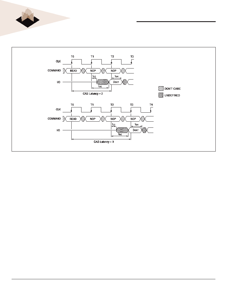
CAS LATENCY
The CAS latency is the delay, in clock cycles, between
the registration of a READ command and the availability
of the rst piece of output data. The latency can be set to
two or three clocks.
If a READ command is registered at clock edge n, and
the latency is m clocks, the data will be available by clock
edge n+m. The I/Os will start driving as a result of the clock
FIGURE 4 – CAS LATENCY
edge one cycle earlier (n + m - 1), and provided that the
relevant access times are met, the data will be valid by
clock edge n + m. For example, assuming that the clock
cycle time is such that all relevant access times are met,
if a READ command is registered at T0 and the latency is
programmed to two clocks, the I/Os will start driving after
T1 and the data will be valid by T2. Table 2 indicates the
operating frequencies at which each CAS latency setting
can be used.
Reserved states should not be used as unknown operation
or incompatibility with future versions may result.
OPERATING MODE
The normal operating mode is selected by setting M7and
M8 to zero; the other combinations of values for M7 and
M8 are reserved for future use and/or test modes. The
programmed burst length applies to both READ and
WRITE bursts.
Test modes and reserved states should not be used
because unknown operation or incompatibility with future
versions may result.
相關(guān)PDF資料 |
PDF描述 |
|---|---|
| W25X32-VSSI-Z | 32M X 1 FLASH 2.7V PROM, PDSO8 |
| WF1024K32E-150H2M | 4M X 8 FLASH 12V PROM MODULE, 150 ns, CHIP66 |
| WS128K48-20G4WMA | 768K X 8 MULTI DEVICE SRAM MODULE, 20 ns, CQFP116 |
| WSF512K32-39G2TMA | SPECIALTY MEMORY CIRCUIT, CQFP68 |
| WS512K16-35DLIA | 512K X 16 MULTI DEVICE SRAM MODULE, 35 ns, CDMA44 |
相關(guān)代理商/技術(shù)參數(shù) |
參數(shù)描述 |
|---|---|
| WEDPN16M64VR-100B2C | 制造商:WEDC 制造商全稱:White Electronic Designs Corporation 功能描述:16Mx64 REGISTERED SYNCHRONOUS DRAM |
| WEDPN16M64VR-100B2I | 制造商:WEDC 制造商全稱:White Electronic Designs Corporation 功能描述:16Mx64 REGISTERED SYNCHRONOUS DRAM |
| WEDPN16M64VR-100B2M | 制造商:WEDC 制造商全稱:White Electronic Designs Corporation 功能描述:16Mx64 REGISTERED SYNCHRONOUS DRAM |
| WEDPN16M64VR-100BC | 制造商:Microsemi Corporation 功能描述:16M X 64 SDRAM MODULE W/REGISTERED BUFFERS, 3.3V, 100 MHZ, 2 - Bulk |
| WEDPN16M64VR-100BI | 制造商:Microsemi Corporation 功能描述:16M X 64 SDRAM MODULE W/REGISTERED BUFFERS, 3.3V, 100 MHZ, 2 - Bulk |
發(fā)布緊急采購,3分鐘左右您將得到回復(fù)。