- 您現(xiàn)在的位置:買(mǎi)賣(mài)IC網(wǎng) > PDF目錄140370 > WEDPZ512K72V-100BC (WHITE ELECTRONIC DESIGNS CORP) 512K X 72 ZBT SRAM, 5 ns, PBGA152 PDF資料下載
參數(shù)資料
| 型號(hào): | WEDPZ512K72V-100BC |
| 廠(chǎng)商: | WHITE ELECTRONIC DESIGNS CORP |
| 元件分類(lèi): | SRAM |
| 英文描述: | 512K X 72 ZBT SRAM, 5 ns, PBGA152 |
| 封裝: | 17 X 23 MM, PLASTIC, BGA-152 |
| 文件頁(yè)數(shù): | 11/15頁(yè) |
| 文件大小: | 0K |
| 代理商: | WEDPZ512K72V-100BC |
第1頁(yè)第2頁(yè)第3頁(yè)第4頁(yè)第5頁(yè)第6頁(yè)第7頁(yè)第8頁(yè)第9頁(yè)第10頁(yè)當(dāng)前第11頁(yè)第12頁(yè)第13頁(yè)第14頁(yè)第15頁(yè)
5
White Electronic Designs Corporation (602) 437-1520 www.wedc.com
White Electronic Designs
WEDPZ512K72V-XBX
February 2009
Rev. 9
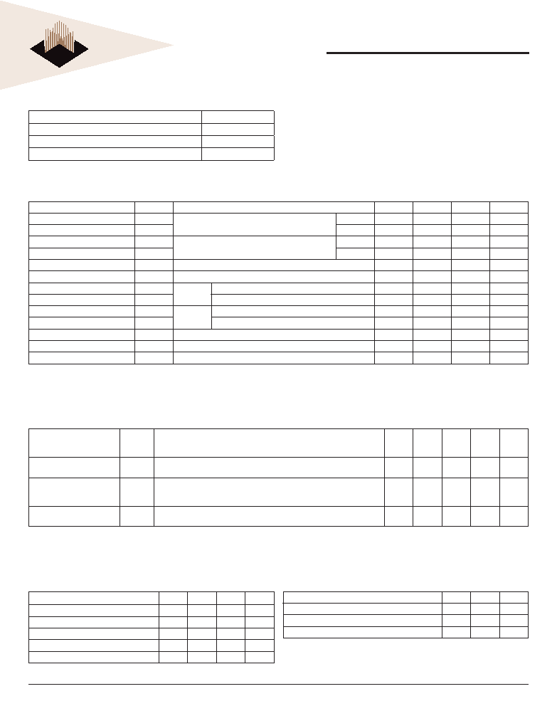
DC CHARACTERISTICS
-55°C ≤ TA ≤ + 125°C
Description
Symbol Conditions
150
MHz
(Max)
133
MHz
(Max)
100
MHz
(Max)
Units
Notes
Power Supply Current:
Operating
IDD
Device Selected; All Inputs ≤ VIL or ≥ VIH; Cycle Time ≥ TCYC MIN;
VCC = MAX; Output Open
700
650
600
mA
1
Power Supply Current:
Standby
ISB2
Device Deselected; VCC = MAX; All Inputs ≤ VIL or ≥ VIH
All Inputs Static; CLK Frequency = MAX
Output Open, ZZ ≥ VCC - 0.2V
300
mA
Clock Running Standby
Current
ISB
Device Deselected; VCC = MAX; All Inputs
≤ VSS + 0.2 or ≥ VCC - 0.2; f = max ; ZZ ≤ VIL
400
mA
NOTES:
1.
IDD is specied with no output current and increases with faster cycle times.
IDD increases with faster cycle times and greater output loading.
ABSOLUTE MAXIMUM RATINGS*
Electrical Characteristics
-55°C ≤ TA ≤ + 125°C
Description
Symbol
Conditions
Min
Max
Units
Notes
Input High (Logic 1) Voltage
VIH
3.3V I/O
2.0
VCC +0.3
V
1
2.5V I/O
1.7
VCC +0.3
Input Low (Logic 0) Voltage
VIL
3.3V I/O
-0.3
0.8
V
1
2.5 I/O
-0.3
0.7
Input Leakage Current
IIL
VCC = Max, 0V ≤ VIN ≤ VCC
-10
+10
μA2
Output Leakage Current
IOL
Output(s) Disabled, VOUT = VSS to VCCQ
-5
+5
μA
Output High Voltage
VOH
IOH = -2.0mA (3.3V I/O)
2.4
—
V
1
IOH = -1mA (2.5v I/O)
2.0
—
V
Output Low Voltage
VOL
IOL = 6.0mA (3.3V I/O)
—
0.4
V
1
IOL = 1.0 mA (2.5v I/O)
—
0.4
V
Supply Voltage
VCC
3.135
3.465
V
1
I/O Power Supply (3.3V)
VCCQ
3.135
3.465
V
1
I/O Power Supply (2.5V)
VCCQ
2.375
2.9
V
1
NOTES:
1.
All voltages referenced to VSS (GND)
2.
LBO# pin has an internal pull-up, and input leakage = ± 200 μA.
BGA CAPACITANCE
TA = + 25°C, f = 1MHz
Description
Symbol Max
Units Notes
Control Input Capacitance (LBO#, zz)
CIC
16
pF
1
Control Input Capacitance
CI
8
pF
1
Input/Output Capacitance (DQ)
CO
10
pF
1
Address Capacitance
CA
16
pF
1
Clock Capacitance
CCK
6
pF
1
NOTES: 1. This parameter is not tested but guaranteed by design.
THERMAL RESISTANCE
Parameter
Symbol
Max
Unit
Thermal Resistance: Die Junction to Ambient
θJA
TBD
°C/W
Thermal Resistance: Die Junction to Ball
θJB
TBD
°C/W
Thermal Resistance: Die Junction to Case
θJC
TBD
°C/W
Note: Refer to Application Note “PBGA Thermal Resistance Corrleation” for further
information regarding WEDC’s thermal modeling.
VIN Voltage or any other pin relative hovss
-0.3V to +4.6V
Voltage on VCC Supply Relative to VSS
-0.3V to +4.6V
Storage Temperature (BGA)
-55°C to +150°C
Maximum Operating Junction Temperature
125°C
* Stress greater than those listed under “Absolute Maximum Ratings: may cause
permanent damage to the device. This is a stress rating only and functional operation
of the device at these or any other conditions greater than those indicated in the
operational sections of this specication is not implied. Exposure to absolute maximum
rating conditions for extended periods may affect reliability.
相關(guān)PDF資料 |
PDF描述 |
|---|---|
| WS128K32-20G1UC | 128K X 32 MULTI DEVICE SRAM MODULE, 20 ns, CQFP68 |
| WS128K32-25G1TCA | 128K X 32 MULTI DEVICE SRAM MODULE, 25 ns, CQFP68 |
| WS128K32-25G1TQA | 128K X 32 MULTI DEVICE SRAM MODULE, 25 ns, CQFP68 |
| WS128K32-35G1UM | 128K X 32 MULTI DEVICE SRAM MODULE, 35 ns, CQFP68 |
| WS128K32-55G1TMA | 128K X 32 MULTI DEVICE SRAM MODULE, 55 ns, CQFP68 |
相關(guān)代理商/技術(shù)參數(shù) |
參數(shù)描述 |
|---|---|
| WEDPZ512K72V-100BI | 制造商:Microsemi Corporation 功能描述:512K X 72 ZBL SSRAM MODULE, 3.3V, 100MHZ, 152 BGA 17MM X 23M - Bulk |
| WEDPZ512K72V-100BM | 制造商:Microsemi Corporation 功能描述:512K X 72 ZBL SSRAM MODULE, 3.3V, 100MHZ, 152 BGA 17MM X 23M - Bulk |
| WEDPZ512K72V-133BC | 制造商:Microsemi Corporation 功能描述:512K X 72 ZBL SSRAM MODULE, 3.3V, 133MHZ, 152 BGA 17MM X 23M - Bulk |
| WEDPZ512K72V-133BI | 制造商:Microsemi Corporation 功能描述:512K X 72 ZBL SSRAM MODULE, 3.3V, 133MHZ, 152 BGA 17MM X 23M - Bulk |
| WEDPZ512K72V-133BM | 制造商:Microsemi Corporation 功能描述:512K X 72 ZBL SSRAM MODULE, 3.3V, 133MHZ, 152 BGA 17MM X 23M - Bulk |
發(fā)布緊急采購(gòu),3分鐘左右您將得到回復(fù)。