- 您現(xiàn)在的位置:買賣IC網(wǎng) > PDF目錄361848 > WF1M32B-150HM3 1Mx32 3.3V Flash Module PDF資料下載
參數(shù)資料
| 型號: | WF1M32B-150HM3 |
| 英文描述: | 1Mx32 3.3V Flash Module |
| 中文描述: | 1Mx32 3.3V的閃存模塊 |
| 文件頁數(shù): | 1/13頁 |
| 文件大小: | 492K |
| 代理商: | WF1M32B-150HM3 |
1
White Electronic Designs Corporation (602) 437-1520 www.wedc.com
White Electronic Designs
WF1M32B-XXX3
March 2006
Rev. 5
White Electronic Designs Corp. reserves the right to change products or specifications without notice.
1Mx32 3.3V Flash Module
FEATURES
Access Times of 100, 120, 150ns
■
Packaging
66 pin, PGA Type, 1.185" square, Hermetic
Ceramic HIP (Package 401)
68 lead, Low Profile CQFP (G2T), 4.6mm
(0.180") square (Package 509)
■
1,000,000 Erase/Program Cycles
■
Sector Architecture
One 16KByte, two 8KBytes, one 32KByte, and
fifteen 64kBytes in byte mode
Any combination of sectors can be concurrently
erased. Also supports full chip erase
■
Organized as 1Mx32
■
Commercial, Industrial and Military Temperature
Ranges
■
3.3 Volt for Read and Write Operations
■
■
■
■
■
Boot Code Sector Architecture (Bottom)
Low Power CMOS, 1.0mA Standby
Embedded Erase and Program Algorithms
Built-in Decoupling Caps for Low Noise Operation
Erase Suspend/Resume
Supports reading data from or programing data to
a sector not being erased
Low Current Consumption
Typical values at 5MHz:
40mA Active Read Current
80mA Program/Erase Current
Weight
WF1M32B-XG2TX3 -8 grams typical
WF1M32B-XHX3 -13 grams typical
Note: For programming information refer to Flash Programming 8M3 Application Note.
■
■
I/O
8
I/O
9
I/O
10
A
14
A
16
A
11
A
0
A
18
I/O
0
I/O
1
I/O
2
RESET#
CS
2
#
GND
I/O
11
A
10
A
9
A
15
V
CC
CS
1
#
A
19
I/O
3
I/O
15
I/O
14
I/O
13
I/O
12
OE#
A
17
WE#
I/O
7
I/O
6
I/O
5
I/O
4
I/O
24
I/O
25
I/O
26
A
7
A
12
NC
A
13
A
8
I/O
16
I/O
17
I/O
18
V
CC
CS
4
#
NC
I/O
27
A
4
A
5
A
6
NC
CS
3
#
GND
I/O
19
I/O
31
I/O
30
I/O
29
I/O
28
A
1
A
2
A
3
I/O
23
I/O
22
I/O
21
I/O
20
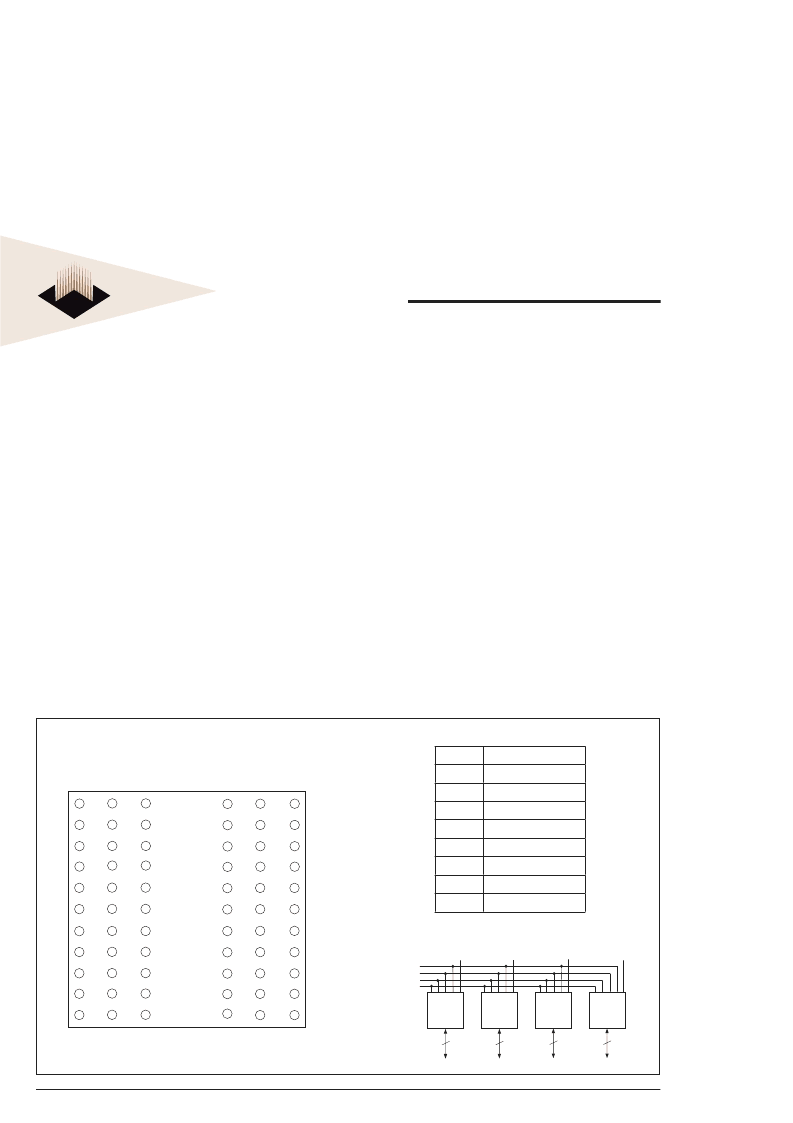
11 22 33 44 55 66
1 12 23 34 45 56
PIN CONFIGURATION FOR WF1M32B-XHX3
Top View
Pin Description
I/O0-31
Data Inputs/Outputs
A0-19
Address Inputs
WE#
Write Enable
CS1-4#
Chip Selects
OE#
Output Enable
RESET#
Reset
V
CC
Power Supply
GND
Ground
NC
Not Connected
Block Diagram
CS1#
CS2#
1M x 8
8
I/O0-7
1M x 8
8
I/O8-15
1M x 8
8
I/O16-23
CS3#
1M x 8
8
I/O24-31
CS4#
AOE#
WE#
RESET#
相關(guān)PDF資料 |
PDF描述 |
|---|---|
| WF1M32B-150HM3A | 1Mx32 3.3V Flash Module |
| WF1M32B-XXX3 | 1Mx32 3.3V Flash Module |
| WF1 | ASSEMBLY JIG PCB ALUMINIUM |
| WF2 | ASSEMBLY JIG PCB ALUMINIUM |
| WFO | ASSEMBLY JIG PCB ALUMINIUM |
相關(guān)代理商/技術(shù)參數(shù) |
參數(shù)描述 |
|---|---|
| WF1M32B-150HM3A | 制造商:WEDC 制造商全稱:White Electronic Designs Corporation 功能描述:1Mx32 3.3V Flash Module |
| WF1M32BP-100G2TI5A | 制造商:未知廠家 制造商全稱:未知廠家 功能描述:x32 Flash EEPROM Module |
| WF1M32BP-100G2TM5A | 制造商:未知廠家 制造商全稱:未知廠家 功能描述:x32 Flash EEPROM Module |
| WF1M32BP-120G2TI5A | 制造商:未知廠家 制造商全稱:未知廠家 功能描述:x32 Flash EEPROM Module |
| WF1M32BP-120G2TM5A | 制造商:未知廠家 制造商全稱:未知廠家 功能描述:x32 Flash EEPROM Module |
發(fā)布緊急采購,3分鐘左右您將得到回復(fù)。