- 您現(xiàn)在的位置:買賣IC網(wǎng) > PDF目錄62768 > WJA1030 SPECIALTY TELECOM CIRCUIT, PSSO3 PDF資料下載
參數(shù)資料
| 型號: | WJA1030 |
| 元件分類: | 通信及網(wǎng)絡(luò) |
| 英文描述: | SPECIALTY TELECOM CIRCUIT, PSSO3 |
| 封裝: | GREEN, SOT-89, 3 PIN |
| 文件頁數(shù): | 1/4頁 |
| 文件大?。?/td> | 185K |
| 代理商: | WJA1030 |
Specifications and information are subject to change without notice
WJ Communications, Inc
Phone 1-800-WJ1-4401 FAX: 408-577-6621 e-mail: sales@wj.com Web site: www.wj.com
Page 1 of 4
Dec 2007
WJA1030
+5V Active-Bias InGaP HBT Gain Block
Product Features
Cascadable gain block
50 – 4000 MHz
15 dB Gain @ 1.9GHz
+18 dBm P1dB @ 1.9GHz
+37 dBm OIP3 @ 1.9GHz
Operates from +5V @ 80mA
0.2dB gain flatness from 0.3-2.5GHz
Robust 1000V ESD, Class 1C
RoHS-compliant SOT-89 package
Applications
Wireless Infrastructure
General Purpose
Cellular GSM, PCS, UMTS
W-CDMA, TD-SCDMA, WiMAX
Product Description
The WJA1030 is a cascadable gain block that offers high
linearity in a low-cost surface-mount package. At 1.9 GHz,
the WJA1030 typically provides 15 dB gain, +37 dBm
OIP3, and +18 dBm P1dB. The device is housed in a
RoHS-compliant SOT-89 industry-standard SMT package
using a NiPdAu plating to eliminate the possibility of tin
whiskering.
The WJA1030 consists of Darlington pair amplifiers using
a high reliability InGaP/GaAs HBT process technology.
The MMIC amplifier is internally matched to 50 and only
requires DC-blocking capacitors and a bias inductor for
operation. An internal active bias is designed to enable
stable performance over temperature. A dropping bias
resistor is not required allowing the device to be biased
directly from a +5V supply voltage.
The broadband amplifier can be directly applied to various
current and next generation wireless technologies such as
GSM, CDMA, W-CDMA, WiBro, and WiMAX. The
WJA1030 is ideal for general purpose applications such as
LO buffering, IF amplification and pre-driver stages within
the 50 to 4000 MHz frequency range.
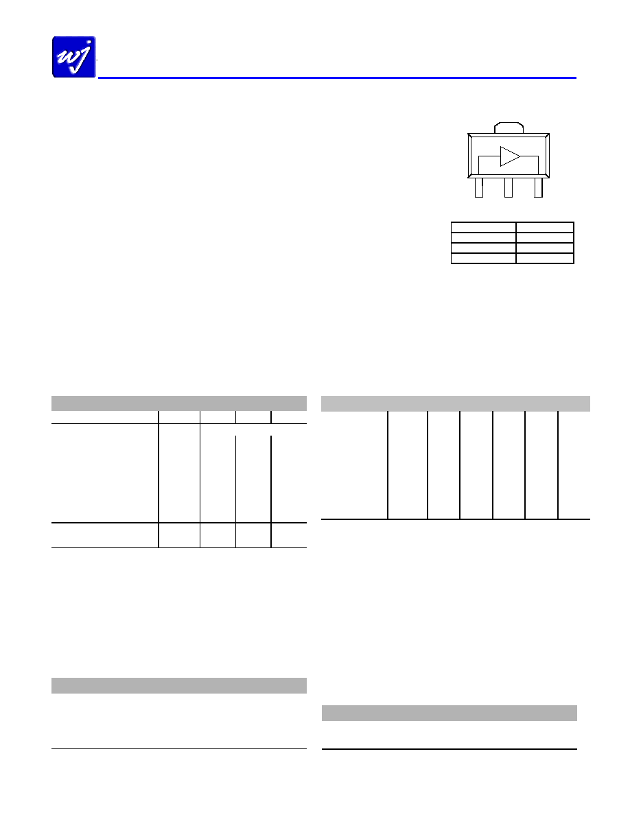
Functional Diagram
RF IN
GND
RF OUT
GND
1
23
4
Function
Pin No.
Input
1
Output/Bias
3
Ground
2, 4
Specifications
(1)
Parameter
Units
Min
Typ
Max
Operational Bandwidth
MHz
50
4000
Test Frequency
MHz
1900
Gain
dB
14.9
Input Return Loss
dB
12
Output Return Loss
dB
16
Output P1dB
dBm
+18.3
Output IP3 (2)
dBm
+37
Output IP2
dBm
+44
Noise Figure
dB
6.1
Device Voltage
V
5
Device Current
mA
80
1. Test conditions: 25 C, Supply Voltage = +5 V, 50
Ω System.. S-parameters and 3OIP measured at
device pins. All other specifications measured on evaluation board.
2. 3OIP measured with two tones at an output power of 3 dBm/tone separated by 1 MHz. The
suppression on the largest IM3 product is used to calculate the 3OIP using a 2:1 rule.
Absolute Maximum Rating
Parameter
Rating
Storage Temperature
-55 to +150
°C
Supply Voltage
+6.5 V
Input Power
+24 dBm
θjc (junction to paddle)
80.6
°C / W
Maximum Junction Temperature
150
°C
Operation of this device above any of these parameters may cause permanent damage.
Typical Performance
(3)
Parameter
Units
Typical
Frequency
MHz
500
900
1900
2140
2500
S21
dB
14.4
14.3
S11
dB
-13
-15
-30
-36
-33
S22
dB
-16
-19
-13
-12
-13
Output P1dB
dBm
+19.4
+19.3
+18.3
+17.5
+16
Output IP3 (2)
dBm
+37.9
+37
+36.6
+36.3
+33.9
Output IP2
dBm
+49.4
+48.3
+44
+41.4
+39.2
Noise Figure
dB
5.3
5.5
6.1
6.3
6.5
3. Listed typical performance parameters measured on evaluation board.
Ordering Information
Part No.
Description
WJA1030
+5V Active Bias InGaP HBT Gain Block
(lead-free/green/RoHS-compliant SOT-89 Package)
WJA1030-PCB
50 – 4000 MHz Fully Assembled Eval. Board
Standard tape / reel size = 1000 pieces on a 7
″ reel
相關(guān)PDF資料 |
PDF描述 |
|---|---|
| WJM1000 | SPECIALTY TELECOM CIRCUIT, SMA15 |
| WJR7080 | SPECIALTY TELECOM CIRCUIT, XMA68 |
| WJS-6D-2.0MADC | POWER/SIGNAL RELAY, DPDT, MOMENTARY, 0.003A (COIL), 30VDC (COIL), 90mW (COIL), 3A (CONTACT), 29VDC (CONTACT), PANEL MOUNT |
| WJS-6D-2.3MADC | POWER/SIGNAL RELAY, DPDT, MOMENTARY, 0.003A (COIL), 24VDC (COIL), 72mW (COIL), 3A (CONTACT), 29VDC (CONTACT), PANEL MOUNT |
| WJS-6D-2.8MADC | POWER/SIGNAL RELAY, DPDT, MOMENTARY, 0.004A (COIL), 20VDC (COIL), 80mW (COIL), 3A (CONTACT), 29VDC (CONTACT), PANEL MOUNT |
相關(guān)代理商/技術(shù)參數(shù) |
參數(shù)描述 |
|---|---|
| WJA1030-PCB | 功能描述:射頻開發(fā)工具 50-2400MHz Eval Brd 15dB Gain RoHS:否 制造商:Taiyo Yuden 產(chǎn)品:Wireless Modules 類型:Wireless Audio 工具用于評估:WYSAAVDX7 頻率: 工作電源電壓:3.4 V to 5.5 V |
| WJA1030TR | 制造商:TriQuint Semiconductor 功能描述:GAIN BLOCK |
| WJA1035 | 功能描述:射頻放大器 50-4000MHz +16dBm P1dB RoHS:否 制造商:Skyworks Solutions, Inc. 類型:Low Noise Amplifier 工作頻率:2.3 GHz to 2.8 GHz P1dB:18.5 dBm 輸出截獲點(diǎn):37.5 dBm 功率增益類型:32 dB 噪聲系數(shù):0.85 dB 工作電源電壓:5 V 電源電流:125 mA 測試頻率:2.6 GHz 最大工作溫度:+ 85 C 安裝風(fēng)格:SMD/SMT 封裝 / 箱體:QFN-16 封裝:Reel |
| WJA1035-PCB | 功能描述:射頻開發(fā)工具 50-2400MHz Eval Brd 15dB Gain RoHS:否 制造商:Taiyo Yuden 產(chǎn)品:Wireless Modules 類型:Wireless Audio 工具用于評估:WYSAAVDX7 頻率: 工作電源電壓:3.4 V to 5.5 V |
| WJA1035TR | 制造商:TriQuint Semiconductor 功能描述:GAIN BLOCK |
發(fā)布緊急采購,3分鐘左右您將得到回復(fù)。