- 您現(xiàn)在的位置:買賣IC網(wǎng) > PDF目錄245652 > WV3HG128M72EER534D7MG (MICROSEMI CORP-PMG MICROELECTRONICS) 128M X 72 DDR DRAM MODULE, 0.5 ns, DMA244 PDF資料下載
參數(shù)資料
| 型號(hào): | WV3HG128M72EER534D7MG |
| 廠商: | MICROSEMI CORP-PMG MICROELECTRONICS |
| 元件分類: | DRAM |
| 英文描述: | 128M X 72 DDR DRAM MODULE, 0.5 ns, DMA244 |
| 封裝: | ROHS COMPLIANT, MINIDIMM-244 |
| 文件頁(yè)數(shù): | 8/11頁(yè) |
| 文件大小: | 200K |
| 代理商: | WV3HG128M72EER534D7MG |
WV3HG128M72EER-D7
October 2006
Rev. 1
ADVANCED
6
White Electronic Designs Corporation (602) 437-1520 www.whiteedc.com
White Electronic Designs
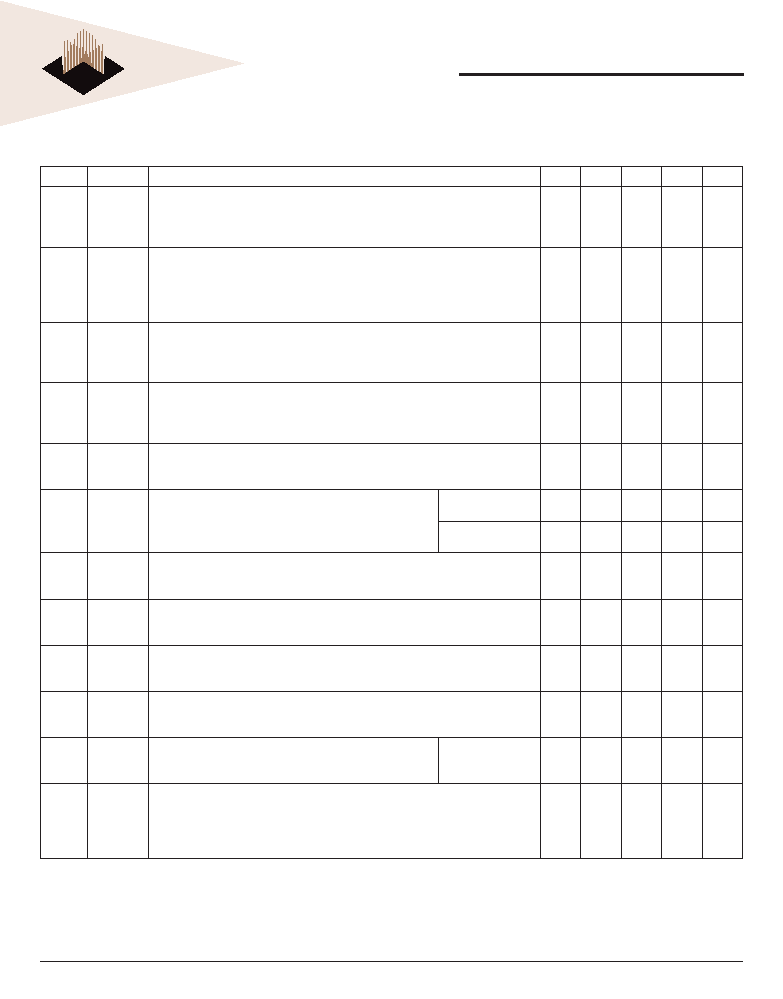
DDR2 ICC SPECIFICATIONS AND CONDITIONS
VCC = +1.8V ± 0.1V
Symbol Parameter Condition
806
665
534
403
Unit
ICC0*
Operating
one bank
active-
precharge;
tCK = tCK(ICC); tRC = tRC(ICC); tRAS = tRAS MIN(ICC); CKE is HIGH, CS# is HIGH between valid
commands; Address bus inputs are SWITCHING; Data bus inputs are SWITCHING
TBD
1,210
1,165
1,120
mA
ICC1*
Operating
one bank
active-
read-
precharge;
IOUT = 0mA; BL = 4; CL = CL(ICC); tCK = tCK(ICC); tRC = tRC(ICC); tRAS = tRAS MIN(ICC); CKE is
HIGH, CS# is HIGH between valid commands; Address bus inputs are SWITCHING;
Data bus inputs are SWITCHING; Data pattern is same as ICC4W.
TBD
1,300
1,255
1,210
mA
ICC2P**
Precharge
power-
down
current;
All banks idle; tCK = tCK(ICC); CKE is LOW; Other control and address bus inputs are
STABLE; Data bus inputs are FLOATING
TBD
508
mA
ICC2Q**
Precharge
quite
standby
current;
All banks idle; tCK = tCK(ICC); CKE is HIGH; CS# is HIGH; Other control and address bus
inputs are STABLE; Data bus inputs are FLOATING
TBD
760
715
mA
ICC2N**
Precharge
standby
current;
All banks idle; tCK = tCK(ICC); CKE is HIGH; CS# is HIGH; Other control and address bus
inputs are STABLE; Data bus inputs are SWITCHING
TBD
805
760
mA
ICC3P**
Active
power-
down
current;
All banks open; tCK = tCK(ICC), CKE is LOW; Other control
and address bus inputs are STABLE; Data bus inputs are
FLOATING
Fast PDN Exit
MRS(12) = 0
TBD
670
625
mA
Slow PDN Exit
MRS(12) = 1
TBD
508
mA
ICC3N**
Active
standby
current;
All banks open; tCK = tCK(ICC); tRC = tRC(ICC); tRAS = tRAS MIN(ICC); CKE is HIGH, CS#
is HIGH between valid commands; Other control and address bus inputs are
SWITCHING; Data bus inputs are SWITCHING
TBD
850
805
mA
ICC4W*
Operating
burst write
current;
All banks open; Continuous burst writes; BL = 4; CL = CL(ICC); AL = 0; tCK = tCK(ICC);
tRC = tRC(ICC); tRAS = tRAS MIN(ICC); CKE is HIGH, CS# is HIGH between valid commands;
Address bus inputs are SWITCHING; Data bus inputs are SWITCHING
TBD
1,795
1,570
1,435
mA
ICC4R*
Operating
burst read
current;
All banks open; Continuous burst reads; TOUT = 0mA; BL = 4; CL = CL(ICC); AL = 0;
tCK = tCK(ICC); tRC = tRC(ICC); tRAS = tRAS MIN(ICC); CKE is HIGH, CS# is HIGH between
valid commands; Address bus inputs are SWITCHING; Data pattern is same as ICC4W.
TBD
1,795
1,570
1,435
mA
ICC5**
Burst auto
refresh
current;
tCK = tCK(ICC); Refresh command at every tRC(ICC) interval; CKE is HIGH; CS# is HIGH
between valid commands; Other control and address bus inputs are SWITCHING;
Data bus inputs are SWITCHING
TBD
2,380
2,335
2,290
mA
ICC6**
Self
refresh
current;
CK and CK# at 0V; CKE < 0.2V; Other control and address bus
inputs are FLOATING; Data bus inputs are FLOATING
Normal
TBD
90
mA
ICC7*
Operating
bank
interleave
read
current;
All bank interleaving reads; IOUT = 0mA; BL = 4; CL = CL(ICC); AL = tRCD(ICC) - 1*tCK(ICC);
tCK = tCK(ICC); tRC = tRC(ICC); tRRD = tRRD MIN(ICC) = 1*tCK(ICC); CKE is HIGH; CS# is HIGH
between valid commands; Address bus inputs are STABLE during DESELECTs; Data
bus inputs are SWITCHING
TBD
3,100
2,920
2,740
mA
Notes:
ICC specication is based on
SAMSUNG components. Other DRAM manufacturers specication may be different.
* Value calculated as one module rank in this operating condition, and all other module ranks in ICC2P ( CKE LOW) mode.
** Value calculated reects all module ranks in this operating condition.
相關(guān)PDF資料 |
PDF描述 |
|---|---|
| WV3HG264M72EEU806D7MG | 128M X 72 DDR DRAM MODULE, DMA244 |
| WS57C71C-55DMB | 32K X 8 UVPROM, 55 ns, CDIP28 |
| WS57C71C-55J | 32K X 8 OTPROM, 55 ns, PQCC32 |
| WF512K32-120G1UM5 | 512K X 32 FLASH 5V PROM MODULE, 120 ns, CQFP68 |
| WF512K32-70G4M5 | 512K X 32 FLASH 5V PROM MODULE, 70 ns, CQFP68 |
相關(guān)代理商/技術(shù)參數(shù) |
參數(shù)描述 |
|---|---|
| WV3HG128M72EER534D7SG | 制造商:WEDC 制造商全稱:White Electronic Designs Corporation 功能描述:1GB - 128Mx72 DDR2 SDRAM REGISTERED, w/PLL, Mini-DIMM |
| WV3HG128M72EER665D7IMG | 制造商:WEDC 制造商全稱:White Electronic Designs Corporation 功能描述:1GB - 128Mx72 DDR2 SDRAM REGISTERED, w/PLL, Mini-DIMM |
| WV3HG128M72EER665D7ISG | 制造商:WEDC 制造商全稱:White Electronic Designs Corporation 功能描述:1GB - 128Mx72 DDR2 SDRAM REGISTERED, w/PLL, Mini-DIMM |
| WV3HG128M72EER665D7MG | 制造商:WEDC 制造商全稱:White Electronic Designs Corporation 功能描述:1GB - 128Mx72 DDR2 SDRAM REGISTERED, w/PLL, Mini-DIMM |
| WV3HG128M72EER665D7SG | 制造商:WEDC 制造商全稱:White Electronic Designs Corporation 功能描述:1GB - 128Mx72 DDR2 SDRAM REGISTERED, w/PLL, Mini-DIMM |
發(fā)布緊急采購(gòu),3分鐘左右您將得到回復(fù)。