- 您現(xiàn)在的位置:買賣IC網(wǎng) > PDF目錄371198 > X24042S8I-3 Serial E2PROM PDF資料下載
參數(shù)資料
| 型號: | X24042S8I-3 |
| 英文描述: | Serial E2PROM |
| 中文描述: | 串行E2PROM |
| 文件頁數(shù): | 5/15頁 |
| 文件大小: | 62K |
| 代理商: | X24042S8I-3 |

X24042
5
BUS ACTIVITY:
MASTER
SDA LINE
BUS ACTIVITY:
X24042
S
T
A
R
T
SLAVE
ADDRESS
S
S
T
O
P
P
A
C
K
A
C
K
A
C
K
WORD
ADDRESS
DATA
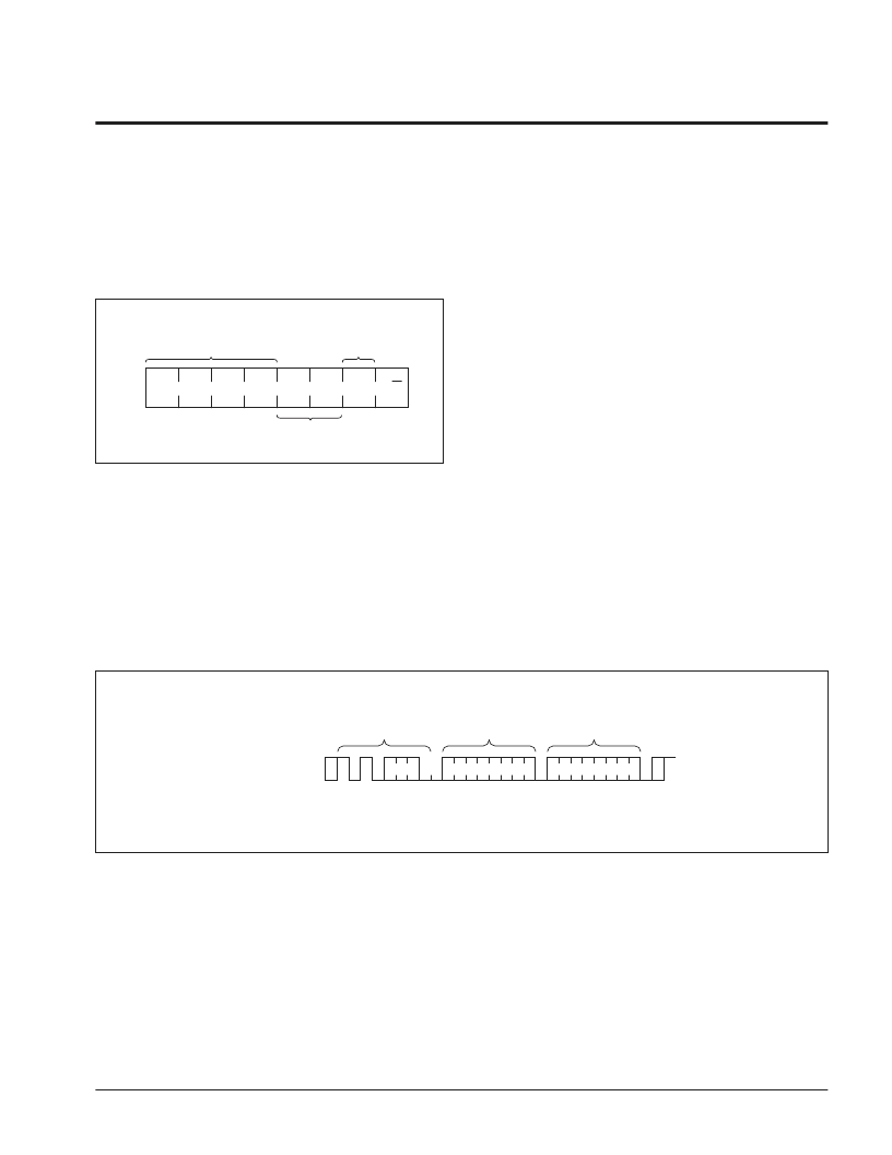
The next two significant bits addresses a particular
device. A system could have up to four X24042 devices
on the bus (see Figure 10). The four addresses are
defined by the state of the A1 and A2 input.
The next bit of the slave address is an extension of the
array’s address and is concatenated with the eight bits
of address in the word address field, providing direct
access to the whole 512 x 8 array.
DEVICE ADDRESSING
Following a start condition the master must output the
address of the slave it is accessing. The most significant
four bits of the slave address are the device type
identifier (see Figure 4). For the X24042 this is fixed as
1010[B].
Figure 4. Slave Address
The last bit of the slave address defines the operation to
be performed. When set to one a read operation is
selected, when set to zero a write operation is selected.
Following the start condition, the X24042 monitors the
SDA bus comparing the slave address being transmit-
ted with its slave address (device type and state of the
A2 and A1 inputs). Upon a correct compare the X24042
outputs an acknowledge on the SDA line. Depending on
the state of the R/
W
bit, the X24042 will execute a read
or write operation.
WRITE OPERATIONS
Byte Write
For a write operation, the X24042 requires a second
address field. This address field is the word address,
comprised of eight bits, providing access to any one of
the 512 words in the selected page of memory. Upon
receipt of the word address the X24042 responds with
an acknowledge, and awaits the next eight bits of data,
again responding with an acknowledge. The master
then terminates the transfer by generating a stop condi-
tion, at which time the X24042 begins the internal write
cycle to the nonvolatile memory. While the internal write
cycle is in progress the X24042 inputs are disabled, and
the device will not respond to any requests from the
master. Refer to Figure 5 for the address, acknowledge
and data transfer sequence.
3849 FHD F09
Figure 5. Byte Write
3849 FHD F10
1
0
A2
A1
A0
R/W
DEVICE TYPE
IDENTIFIER
DEVICE
ADDRESS
1
0
HIGH
ORDER
WORD
ADDRESS
相關PDF資料 |
PDF描述 |
|---|---|
| X24042S8M | Hot Swap Controller IC; Hot Swap Controller Type:Negative Voltage; Controlled Voltage Min:-10V; Controlled Voltage Max:-80V; Number of Controlled Voltages:1; Package/Case:8-SOIC; Power Good Output:Active High |
| X24042S8M-3 | Serial E2PROM |
| X24042PI-2.7 | Serial E2PROM |
| X24042S8-2.7 | Serial E2PROM |
| X24042S8M-2.7 | Serial E2PROM |
相關代理商/技術參數(shù) |
參數(shù)描述 |
|---|---|
| X24042S8M | 制造商:XICOR 制造商全稱:Xicor Inc. 功能描述:Serial E2PROM |
| X24042S8M-2.7 | 制造商:XICOR 制造商全稱:Xicor Inc. 功能描述:Serial E2PROM |
| X24042S8M-3 | 制造商:XICOR 制造商全稱:Xicor Inc. 功能描述:Serial E2PROM |
| X2404DI | 制造商:未知廠家 制造商全稱:未知廠家 功能描述:Serial EEPROM |
| X2404DM | 制造商:未知廠家 制造商全稱:未知廠家 功能描述:Serial EEPROM |
發(fā)布緊急采購,3分鐘左右您將得到回復。