- 您現(xiàn)在的位置:買賣IC網(wǎng) > PDF目錄371199 > X24164PM-2.7 Serial E2PROM PDF資料下載
參數(shù)資料
| 型號(hào): | X24164PM-2.7 |
| 英文描述: | Serial E2PROM |
| 中文描述: | 串行E2PROM |
| 文件頁(yè)數(shù): | 9/14頁(yè) |
| 文件大小: | 60K |
| 代理商: | X24164PM-2.7 |
第1頁(yè)第2頁(yè)第3頁(yè)第4頁(yè)第5頁(yè)第6頁(yè)第7頁(yè)第8頁(yè)當(dāng)前第9頁(yè)第10頁(yè)第11頁(yè)第12頁(yè)第13頁(yè)第14頁(yè)
X24164
9
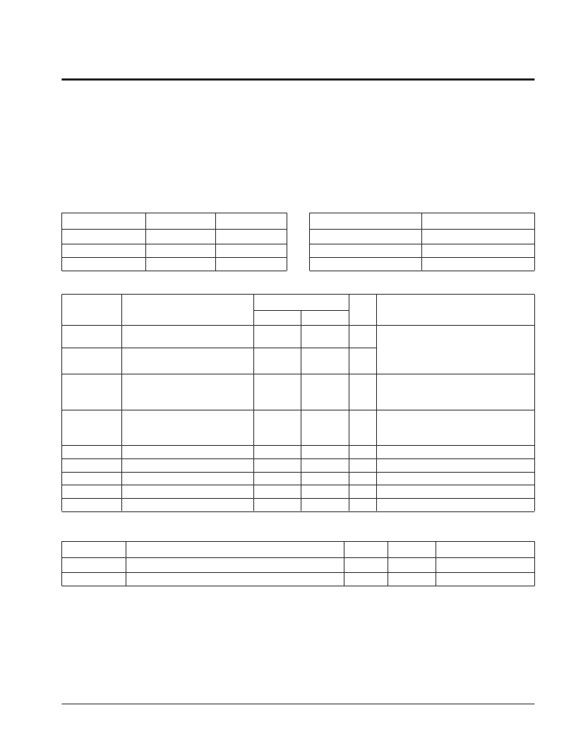
ABSOLUTE MAXIMUM RATINGS*
Temperature Under Bias
X24164 ...................................... –65
°
C to +135
°
C
Storage Temperature ....................... –65
°
C to +150
°
C
Voltage on any Pin with
Respect to V
SS................................
–1.0V to +7.0V
D.C. Output Current ............................................5 mA
Lead Temperature (Soldering, 10 Seconds) ..... 300
°
C
*COMMENT
Stresses above those listed under “Absolute Maximum
Ratings” may cause permanent damage to the device.
This is a stress rating only and the functional operation of
the device at these or any other conditions above those
indicated in the operational sections of this specification is
not implied. Exposure to absolute maximum rating condi-
tions for extended periods may affect device reliability.
RECOMMENDED OPERATING CONDITIONS
Temperature
Min.
0
°
C
–40
°
C
–55
°
C
Max.
70
°
C
+85
°
C
+125
°
C
3846 PGM T02
Commercial
Industrial
Military
Supply Voltage
Limits
X24164
X24164-3
X24164-2.7
4.5V to 5.5V
3V to 5.5V
2.7V to 5.5V
3846 PGM T03
CAPACITANCE
T
A
= 25
°
C, f = 1.0 MHz, V
CC
= 5V
Symbol
C
I/O(3)
Input/Output Capacitance (SDA)
C
IN(3)
Input Capacitance (S
0
, S
1
, S
2
, SCL)
Parameter
Max.
Units
Test Conditions
8
6
pF
pF
V
I/O
= 0V
V
IN
= 0V
3846 PGM T05
Notes:
(1) Must perform a stop command prior to measurement.
(2) V
IL
min. and V
IH
max. are for reference only and are not 100% tested.
(3) This parameter is periodically sampled and not 100% tested.
D.C. OPERATING CHARACTERISTICS
(Over recommended operating conditions unless otherwise specified.)
Limits
Symbol
Parameter
Min.
Max.
Units
Test Conditions
I
CC1
V
CC
Supply Current (Read)
1
mA
SCL = V
CC
X 0.1/V
CC
X 0.9 Levels
@ 100 KHz, SDA = Open, All
Other
I
CC2
I
SB1(1)
V
CC
Supply Current (Write)
V
CC
Standby Current
3
mA
μ
A
Inputs = GND or V
CC
– 0.3V
SCL = SDA = V
CC
, All Other
Inputs = GND or V
CC
– 0.3V,
V
CC
= 5V
±
10%
SCL = SDA = V
CC
, All Other
Inputs = GND or V
CC
– 0.3V,
V
CC
= 3V
V
IN
= GND to V
CC
V
OUT
= GND to V
CC
150
I
SB2(1)
V
CC
Standby Current
50
μ
A
I
LI
I
LO
V
lL(2)
V
IH(2)
V
OL
Input Leakage Current
Output Leakage Current
Input Low Voltage
Input High Voltage
Output Low Voltage
10
10
μ
A
μ
A
V
V
V
–1.0
V
CC
x 0.3
V
CC
x 0.7 V
CC
+ 0.5
0.4
I
OL
= 3 mA
3846 PGM T04
相關(guān)PDF資料 |
PDF描述 |
|---|---|
| X24164PM-3 | Serial E2PROM |
| X24164S8-2.7 | Serial E2PROM |
| X24164S8-3 | Serial E2PROM |
| X24164P-2.7 | Serial E2PROM |
| X24164 | Serial E2PROM |
相關(guān)代理商/技術(shù)參數(shù) |
參數(shù)描述 |
|---|---|
| X24164PM-3 | 制造商:XICOR 制造商全稱:Xicor Inc. 功能描述:Serial E2PROM |
| X24164S8 | 制造商:XICOR 制造商全稱:Xicor Inc. 功能描述:Serial E2PROM |
| X24164S8-2.7 | 制造商:XICOR 制造商全稱:Xicor Inc. 功能描述:Serial E2PROM |
| X24164S8-2.7C7000 | 制造商:未知廠家 制造商全稱:未知廠家 功能描述:I2C Serial EEPROM |
| X24164S8-3 | 制造商:XICOR 制造商全稱:Xicor Inc. 功能描述:Serial E2PROM |
發(fā)布緊急采購(gòu),3分鐘左右您將得到回復(fù)。