- 您現(xiàn)在的位置:買賣IC網(wǎng) > PDF目錄371200 > X24256V14 55V Single N-Channel HEXFET Power MOSFET in a D-Pak package; A IRFR4105Z with Standard Packaging PDF資料下載
參數(shù)資料
| 型號(hào): | X24256V14 |
| 英文描述: | 55V Single N-Channel HEXFET Power MOSFET in a D-Pak package; A IRFR4105Z with Standard Packaging |
| 中文描述: | EEPROM的 |
| 文件頁(yè)數(shù): | 4/18頁(yè) |
| 文件大小: | 144K |
| 代理商: | X24256V14 |
第1頁(yè)第2頁(yè)第3頁(yè)當(dāng)前第4頁(yè)第5頁(yè)第6頁(yè)第7頁(yè)第8頁(yè)第9頁(yè)第10頁(yè)第11頁(yè)第12頁(yè)第13頁(yè)第14頁(yè)第15頁(yè)第16頁(yè)第17頁(yè)第18頁(yè)

X24256
Characteristics subject to change without notice.
4 of 18
Stop Condition
All communications must be terminated by a stop con-
dition, which is a LOW to HIGH transition of SDA when
SCL is HIGH. The stop condition is also used to place
the device into the standby power mode after a read
sequence. A stop condition can only be issued after
the transmitting device has released the bus.
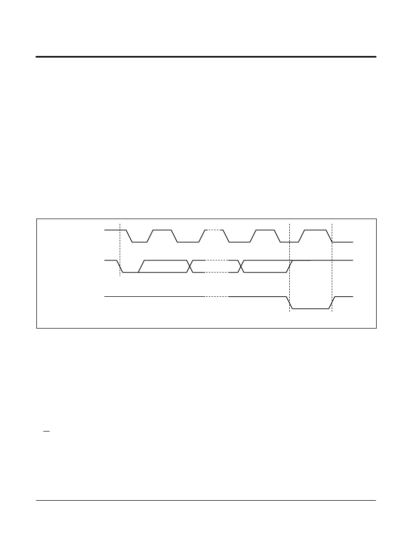
Acknowledge
Acknowledge is a software convention used to indicate
successful data transfer. The transmitting device,
either master or slave, will release the bus after trans-
mitting eight bits. During the ninth clock cycle the
receiver will pull the SDA line LOW to acknowledge
that it received the eight bits of data. Refer to Figure 3.
The device will respond with an acknowledge after rec-
ognition of a start condition and its slave address. If
both the device and a write operation have been
selected, the device will respond with an acknowledge
after the receipt of each subsequent 8-bit word.
In the read mode the device will transmit eight bits of
data, release the SDA line and monitor the line for an
acknowledge. If an acknowledge is detected and no
stop condition is generated by the master, the device
will continue to transmit data. If an acknowledge is not
detected, the device will terminate further data trans-
missions. The master must then issue a stop condition
to return the device to the standby power mode and
place the device into a known state.
Figure 3. Acknowledge Response From Receiver
SCL FROM
MASTER
DATA OUTPUT
FROM
TRANSMITTER
1
8
9
DATA
OUTPUT
FROM
RECEIVER
START
ACKNOWLEDGE
DEVICE ADDRESSING
Following a start condition, the master must output the
address of the slave it is accessing. The first four bits
of the Slave Address Byte are the device type identifier
bits. These must equal “1010”. The next bit is a “0”.
The following 2 bits are the device select bits S
S
1
. This allows up to 4 devices to share a single bus.
These bits are compared to the S
select input pins. The last bit of the Slave Address
Byte defines the operation to be performed. When the
R/W bit is a one, then a read operation is selected.
When it is zero then a write operation is selected.
Refer to Figure 4. After loading the Slave Address
Byte from the SDA bus, the device compares the
device type bits with the value “1010” and the device
select bits with the status of the device select input
0
and
0
and S
1
device
pins. If the compare is not successful, no acknowledge
is output during the ninth clock cycle and the device
returns to the standby mode.
On power up the internal address is undefined, so the
first read or write operation must supply an address.
The word address is either supplied by the master or
obtained from an internal counter, depending on the
operation. The master must supply the two Word
Address Bytes as shown in Figure 4.
The internal organization of the E
by 64 bytes per page. The page address is partially
contained in the Word Address Byte 1 and partially in
bits 7 through 6 of the Word Address Byte 0. The byte
address is contained in bits 5 through 0 of the Word
Address Byte 0. See Figure 4.
2
array is 512 pages
Powered by ICminer.com Electronic-Library Service CopyRight 2003
相關(guān)PDF資料 |
PDF描述 |
|---|---|
| X24256ZI-1.8 | 30V Single N-Channel HEXFET Power MOSFET in a D2-Pak package; A IRL7833S with Standard Packaging |
| X24256ZI-2.5 | EEPROM |
| X24320S8-1.8 | 16 Characters x 2 Lines, 5x7 Dot Matrix Character and Cursor |
| X24320S8-2.5 | 16 Characters x 2 Lines, 5x7 Dot Matrix Character and Cursor |
| X24320V14-2.5 | 400KHz 2-Wire Serial E2PROM with Block Lock |
相關(guān)代理商/技術(shù)參數(shù) |
參數(shù)描述 |
|---|---|
| X24256V14-1.8 | 制造商:未知廠家 制造商全稱:未知廠家 功能描述:EEPROM |
| X24256V14-2.5 | 制造商:未知廠家 制造商全稱:未知廠家 功能描述:I2C Serial EEPROM |
| X24256V14I | 制造商:未知廠家 制造商全稱:未知廠家 功能描述:EEPROM |
| X24256V14I-1.8 | 制造商:未知廠家 制造商全稱:未知廠家 功能描述:EEPROM |
| X24256V14I-2.5 | 制造商:未知廠家 制造商全稱:未知廠家 功能描述:I2C Serial EEPROM |
發(fā)布緊急采購(gòu),3分鐘左右您將得到回復(fù)。