- 您現(xiàn)在的位置:買賣IC網(wǎng) > PDF目錄371201 > X24325V Voltage Regulator IC; Leaded Process Compatible:Yes; Peak Reflow Compatible (260 C):Yes RoHS Compliant: Yes PDF資料下載
參數(shù)資料
| 型號: | X24325V |
| 英文描述: | Voltage Regulator IC; Leaded Process Compatible:Yes; Peak Reflow Compatible (260 C):Yes RoHS Compliant: Yes |
| 中文描述: | 先進的2線串行e的2座門鎖TM保護胎膜早破 |
| 文件頁數(shù): | 5/17頁 |
| 文件大?。?/td> | 79K |
| 代理商: | X24325V |

X24325
5
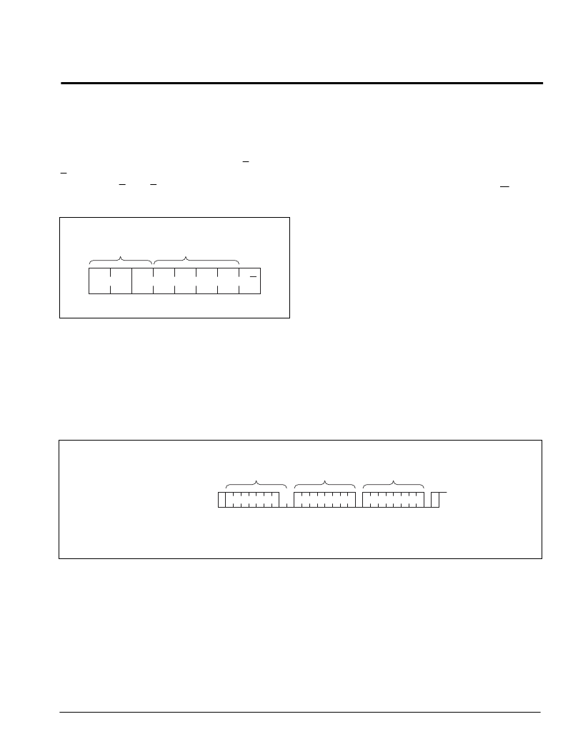
Figure 5. Byte Write
BUS ACTIVITY:
MASTER
SDA LINE
BUS ACTIVITY:
X24325
S
T
A
R
T
SLAVE
ADDRESS
S
S
T
O
P
P
A
C
K
A
C
K
A
C
K
WORD
ADDRESS
DATA
6552 ILL F08
DEVICE ADDRESSING
Following a start condition the master must output the
address of the slave it is accessing (see Figure 4). The
next three bits are the device select bits. A system
could have up to eight X24325’s on the bus. The eight
addresses are defined by the state of the S
S
2
inputs. S
0
and S
2
of the slave address must be the
inverse of the S
0
and S
2
input pins.
0
, S
1
and
Figure 4. Slave Address
The next four bits of the slave address are an exten-
sion of the array’s address and are concatenated with
the eight bits of address in the word address field,
providing direct access to the whole 4096 x 8 array.
6552 ILL F07.2
S2
A9
A8
R/W
DEVICE
SELECT
S1
S0
HIGH ORDER
WORD
ADDRESS
A11
A10
The last bit of the slave address defines the operation to
be performed. When set HIGH a read operation is
selected, when set LOW a write operation is selected.
Following the start condition, the X24325 monitors the
SDA bus comparing the slave address being transmitted
with its slave address device type identifier. Upon a
correct compare the X24325 outputs an acknowledge on
the SDA line. Depending on the state of the R/W bit, the
X24325 will execute a read or write operation.
WRITE OPERATIONS
Byte Write
For a write operation, the X24325 requires a second ad-
dress field. This address field is the word address, com-
prised of eight bits, providing access to any one of 4096
words in the array. Upon receipt of the word address, the
X24325 responds with an acknowledge and awaits the
next eight bits of data, again responding with an acknowl-
edge. The master then terminates the transfer by gener-
ating a stop condition, at which time the X24325 begins
the internal write cycle to the nonvolatile memory. While
the internal write cycle is in progress the X24325 inputs
are disabled, and the device will not respond to any re-
quests from the master. Refer to Figure 5 for the address,
acknowledge and data transfer sequence.
相關PDF資料 |
PDF描述 |
|---|---|
| X24325VI | IC STEP-UP SW REG 2A 10-MLPD |
| X24325VM | Advanced 2-Wire Serial E 2 PROM with Block Lock TM Protection |
| X24325V-2.7 | OSC 5V SMT 7X5 CMOS PROGRM |
| X24325PM-2.7 | Advanced 2-Wire Serial E 2 PROM with Block Lock TM Protection |
| X24640V20I-1.8 | 400KHz 2-Wire Serial E 2 PROM with Block Lock |
相關代理商/技術參數(shù) |
參數(shù)描述 |
|---|---|
| X24325V-2.7 | 制造商:XICOR 制造商全稱:Xicor Inc. 功能描述:Advanced 2-Wire Serial E 2 PROM with Block Lock TM Protection |
| X24325VI | 制造商:XICOR 制造商全稱:Xicor Inc. 功能描述:Advanced 2-Wire Serial E 2 PROM with Block Lock TM Protection |
| X24325VI-2.7 | 制造商:XICOR 制造商全稱:Xicor Inc. 功能描述:Advanced 2-Wire Serial E 2 PROM with Block Lock TM Protection |
| X24325VM | 制造商:XICOR 制造商全稱:Xicor Inc. 功能描述:Advanced 2-Wire Serial E 2 PROM with Block Lock TM Protection |
| X24325VM-2.7 | 制造商:XICOR 制造商全稱:Xicor Inc. 功能描述:Advanced 2-Wire Serial E 2 PROM with Block Lock TM Protection |
發(fā)布緊急采購,3分鐘左右您將得到回復。