- 您現(xiàn)在的位置:買賣IC網(wǎng) > PDF目錄371201 > X24640PI-2.5 400KHz 2-Wire Serial E 2 PROM with Block Lock PDF資料下載
參數(shù)資料
| 型號(hào): | X24640PI-2.5 |
| 英文描述: | 400KHz 2-Wire Serial E 2 PROM with Block Lock |
| 中文描述: | 400kHz的2線串行E的2座鎖胎膜早破 |
| 文件頁數(shù): | 5/17頁 |
| 文件大小: | 85K |
| 代理商: | X24640PI-2.5 |

X24640
5
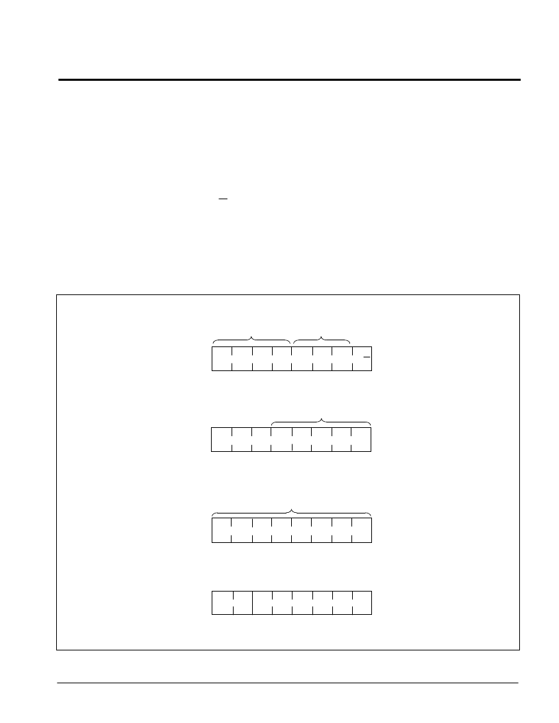
Figure 4. Device Addressing
1
S1
S0
R/W
DEVICE
SELECT
0
1
0
S2
DEVICE TYPE
IDENTIFIER
SLAVE ADDRESS BYTE
D7
D2
D1
D6
D5
D4
D3
DATA BYTE
A2
A1
A0
A5
LOW ORDERWORD ADDRESS
A4
A3
WORD ADDRESS BYTE 0
0
A10
A9
A8
0
HIGH ORDER WORD ADDRESS
A11
X24640WORD ADDRESS BYTE 1
0
A12
A7
A6
D0
7038 FM 06
DEVICE ADDRESSING
Following a start condition, the master must output the
address of the slave it is accessing. The first four bits
of the Slave Address Byte are the device type identifier
bits. These must equal “1010”. The next 3 bits are the
device select bits S
0
, S
1
, and S
devices to share a single bus. These bits are
compared to the S
0
, S
1
, and S
pins. The last bit of the Slave Address Byte defines the
operation to be performed. When the R/W bit is a one,
then a read operation is selected. When it is zero then
a write operation is selected. Refer to figure 4. After
loading the Slave Address Byte from the SDA bus, the
device compares the device type bits with the value
“1010” and the device select bits with the status of the
2
. This allows up to 8
2
device select input
device select input pins. If the compare is not successful,
no acknowledge is output during the ninth clock cycle
and the device returns to the standby mode.
The word address is either supplied by the master or
obtained from an internal counter, depending on the
operation. The master must supply the two Word
Address Bytes as shown in figure 4.
The internal organization of the E
32 bytes per page. The page address is partially
contained in the Word Address Byte 1 and partially in
bits 7 through 5 of the Word Address Byte 0. The byte
address is contained in bits 4 through 0 of the Word
Address Byte 0. See figure 4.
2
array is 256 pages by
發(fā)布緊急采購,3分鐘左右您將得到回復(fù)。