- 您現(xiàn)在的位置:買賣IC網(wǎng) > PDF目錄371202 > X24C00 Serial E2PROM PDF資料下載
參數(shù)資料
| 型號(hào): | X24C00 |
| 英文描述: | Serial E2PROM |
| 中文描述: | 串行E2PROM |
| 文件頁(yè)數(shù): | 4/11頁(yè) |
| 文件大小: | 44K |
| 代理商: | X24C00 |

4
X24C00
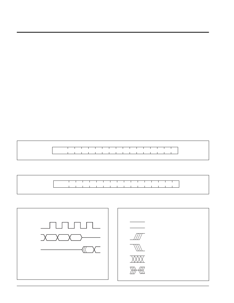
Read Operation
The byte read operation is initiated with a start condition.
The start condition is followed by an eight-bit control byte
which consists of a two-bit read command (1,0), four
address bits, and two “don’t care” bits. After receipt of
the control byte the X24C00 will enter the read mode and
transfer data into the shift register from the array. This
data is shifted out of the device on the next eight SCL
clocks. At the end of the read, all counters are reset and
the X24C00 will enter the standby mode. As with a write,
the read operation can be interrupted by a start or stop
condition while the command or address is being clocked
in. While clocking data out, starts or stops cannot be
generated.
During the second don’t care clock cycle, starts and
stops are ignored. The master must free the bus prior to
the end of this clock cycle to allow the X24C00 to begin
outputting data (Figures 5 and 6).
After receipt of the control byte, the X24C00 will enter
the write mode and await the data to be written. This data
is shifted into the device on the next eight SCL clocks.
Once eight clocks have been received, the data in the
shift register will be written into the memory array. While
the write is in progress the X24C00 will not respond to
any inputs. At any time prior to clocking in the last data
bit, a stop command or a new start command will
terminate the operation. If a start command is given, the
X24C00 will reset all counters and will prepare to clock
in the next control byte. If a stop command is given, the
X24C00 will reset all counters and await the next start
command.
At the end of the write the X24C00 will automatically
reset all counters and enter the standby mode.
(Figure 4).
Figure 4. Write Sequence
3836 FHD F06
START
0
1
A3
A2
A1
A0
XX
XX
D7
D6
D5
D4
D3
D2
D1
D0
Figure 5. Read Sequence
START
1
0
A3
A2
A1
A0
XX
XX
D7
D6
D5
D4
D3
D2
D1
D0
3836 FHD F07
6
7
8
1
SDA IN
SCK
SDA OUT
A0
XX
XX
D7
D6
3836 FHD F08
WAVEFORM
INPUTS
OUTPUTS
Must be
steady
Will be
steady
May change
from LOW
to HIGH
Will change
from LOW
to HIGH
May change
from HIGH
to LOW
Will change
from HIGH
to LOW
Don’t Care:
Changes
Allowed
N/A
Changing:
State Not
Known
Center Line
is High
Impedance
SYMBOL TABLE
Figure 6. Read Cycle Timing
相關(guān)PDF資料 |
PDF描述 |
|---|---|
| X24C00M | Serial E2PROM |
| X24C00M-2.7 | Serial E2PROM |
| X24C00M-3 | Serial E2PROM |
| X24C00MI | Serial E2PROM |
| X24C00MI-3 | Serial E2PROM |
相關(guān)代理商/技術(shù)參數(shù) |
參數(shù)描述 |
|---|---|
| X24C00M | 制造商:XICOR 制造商全稱:Xicor Inc. 功能描述:Serial E2PROM |
| X24C00M-2.7 | 制造商:XICOR 制造商全稱:Xicor Inc. 功能描述:Serial E2PROM |
| X24C00M-3 | 制造商:XICOR 制造商全稱:Xicor Inc. 功能描述:Serial E2PROM |
| X24C00MI | 制造商:XICOR 制造商全稱:Xicor Inc. 功能描述:Serial E2PROM |
| X24C00MI-2.7 | 制造商:XICOR 制造商全稱:Xicor Inc. 功能描述:Serial E2PROM |
發(fā)布緊急采購(gòu),3分鐘左右您將得到回復(fù)。