- 您現(xiàn)在的位置:買賣IC網(wǎng) > PDF目錄371224 > X25F032VI SerialFlash⑩ Memory With Block LockTM Protection PDF資料下載
參數(shù)資料
| 型號: | X25F032VI |
| 英文描述: | SerialFlash⑩ Memory With Block LockTM Protection |
| 中文描述: | SerialFlash⑩帶座LockTM內(nèi)存保護(hù) |
| 文件頁數(shù): | 2/16頁 |
| 文件大小: | 71K |
| 代理商: | X25F032VI |
2
X25F064/032/016/008
Hold (
HOLD
)
HOLD
is used in conjunction with the
CS
pin to select the
device. Once the part is selected and a serial sequence
is underway,
HOLD
may be used to pause the serial
communication with the controller without resetting the
serial sequence. To pause,
HOLD
must be brought
LOW while SCK is LOW. To resume communication,
HOLD
is brought HIGH, again while SCK is LOW. If the
pause feature is not used,
HOLD
should be held HIGH
at all times.
PIN NAMES
SYMBOL
DESCRIPTION
CS
SO
SI
SCK
PP
V
SS
V
CC
HOLD
NC
Chip Select Input
Serial Output
Serial Input
Serial Clock Input
Program Protect Input
Ground
Supply Voltage
Hold Input
No Connect
6685 PGM T01.1
PIN DESCRIPTIONS
Serial Output (SO)
SO is a push-pull serial data output pin. During a read
cycle, data is shifted out on this pin. Data is clocked out
by the falling edge of the serial clock.
Serial Input (SI)
SI is the serial data input pin. All opcodes, byte
addresses, and data to be written to the memory are
input on this pin. Data is latched by the rising edge of the
serial clock.
Serial Clock (SCK)
The Serial Clock controls the serial bus timing for data
input and output. Opcodes, addresses, or data present
on the SI pin are latched on the rising edge of the clock
input, while data on the SO pin change after the falling
edge of the clock input.
Chip Select (
CS
)
When
CS
is HIGH, the X25F064/032/016/008 is
deselected and the SO output pin is at high impedance
and unless an internal program operation is underway
the X25F064/032/016/008 will be in the standby power
mode.
CS
LOW enables the X25F064/032/016/008,
placing it in the active power mode. It should be noted
that after power-up, a HIGH to LOW transition on
CS
is
required prior to the start of any operation.
Program Protect (
PP
)
When
PP
is LOW and the nonvolatile bit PPEN is “1”,
nonvolatile programming of the X25F064/032/016/008
status register is disabled, but the part otherwise func-
tions normally. When
PP
is held HIGH, all functions,
including nonvolatile programming operate normally.
PP
going LOW while
CS
is still LOW will interrupt
programming of the X25F064/032/016/008 status regis-
ter. If the internal program cycle has already been
initiated,
PP
going
LOW
will have no effect on program-
ming.
The
PP
pin function is blocked when the PPEN bit in
the status register is “0”. This allows the user to install the
X25F064/032/016/008 into a system with
PP
pin
grounded and still be able to program the status register.
The
PP
pin functions will be enabled when the PPEN bit
is set “0”.
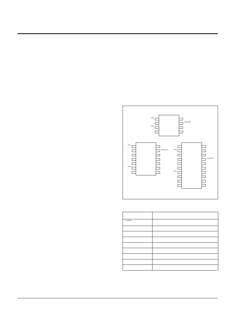
PIN CONFIGURATION
6685 ILL F02.4
CS
SO
PP
VSS
1
2
3
4
8
7
6
5
VCC
HOLD
SCK
SI
8-Lead DIP/SOIC
14-Lead TSSOP
20-Lead TSSOP
CS
SO
NC
NC
NC
PP
VSS
1
2
3
4
5
6
7
VCC
HOLD
NC
NC
NC
SCK
SI
14
13
12
11
10
9
8
NC
CS
NC
SO
NC
NC
PP
VSS
NC
NC
1
2
3
4
5
6
7
8
9
10
NC
VCC
NC
HOLD
NC
NC
SCK
SI
NC
NC
20
19
18
17
16
15
14
13
12
11
X25F064/
032/016/
008
X25F032/
016/008
X25F064
相關(guān)PDF資料 |
PDF描述 |
|---|---|
| X25F064 | SerialFlash⑩ Memory With Block LockTM Protection |
| X25F064P | SerialFlash⑩ Memory With Block LockTM Protection |
| X25F064P-5 | SerialFlash⑩ Memory With Block LockTM Protection |
| X25F064PE | SerialFlash⑩ Memory With Block LockTM Protection |
| X25F064PI | SerialFlash⑩ Memory With Block LockTM Protection |
相關(guān)代理商/技術(shù)參數(shù) |
參數(shù)描述 |
|---|---|
| X25F032VI-5 | 制造商:XICOR 制造商全稱:Xicor Inc. 功能描述:SerialFlash⑩ Memory With Block LockTM Protection |
| X25F047 | 制造商:XICOR 制造商全稱:Xicor Inc. 功能描述:SPI SerialFlash with Block Lock TM Protection |
| X25F047M | 制造商:XICOR 制造商全稱:Xicor Inc. 功能描述:SPI SerialFlash with Block Lock TM Protection |
| X25F047M-5 | 制造商:XICOR 制造商全稱:Xicor Inc. 功能描述:SPI SerialFlash with Block Lock TM Protection |
| X25F047MI | 制造商:XICOR 制造商全稱:Xicor Inc. 功能描述:SPI SerialFlash with Block Lock TM Protection |
發(fā)布緊急采購,3分鐘左右您將得到回復(fù)。