- 您現(xiàn)在的位置:買賣IC網(wǎng) > PDF目錄371263 > X5163 (Intersil Corporation) RTC Module With CPU Supervisor PDF資料下載
參數(shù)資料
| 型號(hào): | X5163 |
| 廠商: | Intersil Corporation |
| 元件分類: | CPU監(jiān)測(cè) |
| 英文描述: | RTC Module With CPU Supervisor |
| 中文描述: | 時(shí)鐘模塊CPU監(jiān)控 |
| 文件頁(yè)數(shù): | 7/21頁(yè) |
| 文件大?。?/td> | 117K |
| 代理商: | X5163 |
第1頁(yè)第2頁(yè)第3頁(yè)第4頁(yè)第5頁(yè)第6頁(yè)當(dāng)前第7頁(yè)第8頁(yè)第9頁(yè)第10頁(yè)第11頁(yè)第12頁(yè)第13頁(yè)第14頁(yè)第15頁(yè)第16頁(yè)第17頁(yè)第18頁(yè)第19頁(yè)第20頁(yè)第21頁(yè)

X5163/X5165 – Preliminary Information
Characteristics subject to change without notice.
7 of 21
REV 1.1 3/5/01
www.xicor.com
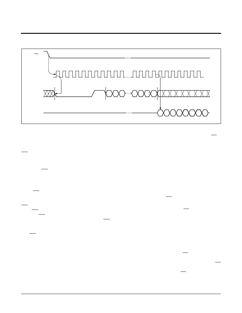
Figure 5. Read EEPROM Array Sequence
0
1
2
3
4
5
6
7
8
9
10
20 21 22 23 24 25
26 27 28 29 30
7
6
5
4
3
2
1
0
Data Out
CS
SCK
SI
SO
MSB
High Impedance
Instruction
16 Bit Address
15 14 13
3
2
1
0
In Circuit Programmable ROM Mode
This mechanism protects the block lock and Watchdog
bits from inadvertent corruption.
In the locked state
(
Programmable ROM Mode) the
WP pin is LOW and the nonvolatile bit WPEN is “1”.
This mode disables nonvolatile writes to the device’s
Status Register.
Setting the WP pin LOW while WPEN is a “1” while an
internal write cycle to the Status Register is in progress
will not stop this write operation, but the operation dis-
ables subsequent write attempts to the Status Register.
When WP is HIGH, all functions, including nonvolatile
writes to the Status Register operate normally. Setting
the WPEN bit in the Status Register to “0” blocks the
WP pin function, allowing writes to the Status Register
when WP is HIGH or LOW. Setting the WPEN bit to “1”
while the WP pin is LOW activates the Programmable
ROM mode, thus requiring a change in the WP pin
prior to subsequent Status Register changes. This
allows manufacturing to install the device in a system
with WP pin grounded and still be able to program the
Status Register. Manufacturing can then load Configu-
ration data, manufacturing time and other parameters
into the EEPROM, then set the portion of memory to
be protected by setting the block lock bits, and finally
set the “OTP mode” by setting the WPEN bit. Data
changes now require a hardware change.
Read Sequence
When reading from the EEPROM memory array, CS is
first pulled low to select the device. The 8-bit READ
instruction is transmitted to the device, followed by the
16-bit address. After the READ opcode and address
are sent, the data stored in the memory at the selected
address is shifted out on the SO line. The data stored
in memory at the next address can be read sequen-
tially by continuing to provide clock pulses. The
address is automatically incremented to the next
higher address after each byte of data is shifted out.
When the highest address is reached, the address
counter rolls over to address $0000 allowing the read
cycle to be continued indefinitely. The read operation is
terminated by taking CS high. Refer to the Read
EEPROM Array Sequence (Figure 1).
To read the Status Register, the CS line is first pulled
low to select the device followed by the 8-bit RDSR
instruction. After the RDSR opcode is sent, the contents
of the Status Register are shifted out on the SO line.
Refer to the Read Status Register Sequence (Figure 2).
Write Sequence
Prior to any attempt to write data into the device, the
“Write Enable” Latch (WEL) must first be set by issuing
the WREN instruction (Figure 3). CS is first taken LOW,
then the WREN instruction is clocked into the device.
After all eight bits of the instruction are transmitted, CS
must then be taken HIGH. If the user continues the
Write Operation without taking CS HIGH after issuing
the WREN instruction, the Write Operation will be
ignored.
相關(guān)PDF資料 |
PDF描述 |
|---|---|
| X51638S8 | RTC Module With CPU Supervisor |
| X5163P | RTC Module With CPU Supervisor |
| X5163P-2.7 | RTC Module With CPU Supervisor |
| X5163P-2.7A | RTC Module With CPU Supervisor |
| X5163P-4.5A | RTC Module With CPU Supervisor |
相關(guān)代理商/技術(shù)參數(shù) |
參數(shù)描述 |
|---|---|
| X5163_06 | 制造商:INTERSIL 制造商全稱:Intersil Corporation 功能描述:CPU Supervisor with 16Kbit SPI EEPROM |
| X51638P | 制造商:未知廠家 制造商全稱:未知廠家 功能描述:SPI Serial EEPROM with Supervisory Features |
| X51638P-4.5A | 制造商:未知廠家 制造商全稱:未知廠家 功能描述:SPI Serial EEPROM with Supervisory Features |
| X51638S8 | 制造商:INTERSIL 制造商全稱:Intersil Corporation 功能描述:CPU Supervisor with 16Kbit SPI EEPROM Description |
| X51638S8-1.8 | 制造商:未知廠家 制造商全稱:未知廠家 功能描述:SPI Serial EEPROM with Supervisory Features |
發(fā)布緊急采購(gòu),3分鐘左右您將得到回復(fù)。