- 您現(xiàn)在的位置:買賣IC網(wǎng) > PDF目錄371269 > X68C75PM Port Expander and E2 Memory PDF資料下載
參數(shù)資料
| 型號: | X68C75PM |
| 英文描述: | Port Expander and E2 Memory |
| 中文描述: | 端口擴展和E2內(nèi)存 |
| 文件頁數(shù): | 2/26頁 |
| 文件大小: | 123K |
| 代理商: | X68C75PM |

2
X68C75 SLIC
E
2
Each bidirectional port consists of 8 general purpose
I/O lines and 1 data strobe line. The ports also feature a
configurable interrupt request output.
Access to the X68C75 is accomplished through the
multiplexed address/data bus of the 68HC11 type con-
trollers. An internal programmable address decoder
maps the internal memory and register locations into the
desired address space.
ARCHITECTURAL OVERVIEW
The X68C75 incorporates the interface circuitry nor-
mally needed to decode the control signals and
demultiplex the address/data bus to provide a “seam-
less” interface.
The control inputs on the X68C75 are configured such
that it is possible to directly connect them to the proper
interface signals of the 68HC11 microcontroller. The
reading of data from the chip is controlled by the
R/
W
and E clock signals.
Reading and writing of the nonvolatile memory array is
analogous to RAM operation. During a write operation to
either the nonvolatile memory or the control registers,
the falling edge of AS latches the address present on the
address bus into the X68C75, and the falling edge of E
clock latches the data to be written.
The nonvolatile memory of the X68C75 is internally
organized as two independent arrays of 4K-bytes with
the A12 input selecting which of the two planes of
memory is to be accessed. While the processor is
executing code out of one plane, write operations can
take place in the other plane; allowing the processor to
continue execution of code out of the X68C75 during a
byte or page write to the device. This feature is called
Concurrent Read During Write.
The X68C75 also features an advanced implementation
of the Software Data Protection scheme, called Block
Protect, which allows the nonvolatile memory array to be
treated as 8 independent sections of 1K-bytes. Each of
these sections can be independently enabled for write
operations. This allows segmentation of the memory
contents into writable and non-writable sections, thereby,
allowing certain sections of the device to be secured so
that updates can only occur in a controlled environ-
ment. (e.g. in an automotive application, only at an
authorized service center). The Block Protect configu-
ration is stored in a nonvolatile register, ensuring that
the configuration data will be maintained after the
device is powered-down.
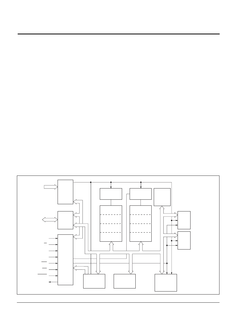
FUNCTIONAL DIAGRAM
2899 ILL F03
ADDRESS
LATCH
I/O
BUFFER
&
LATCH
MASTER
CONTROL
LOGIC
LEFT PLANE
DECODE
RIGHT PLANE
DECODE
1K X 8
1K X 8
E2PROM
CE
AS
SEL
E
R/W
RESET
IRQ
1K X 8
1K X 8
1K X 8
1K X 8
E2PROM
1K X 8
1K X 8
SDP
DECODE
CONFIG
REGISTER
MAP
MEM.
PORT
SPECIAL
FUNCTION
REGISTERS
PORT
A
PORT
B
PORT SELECT
DATA I/O BUS
A0–A15
I/O0–I/O7
WC
16 X 8
GENERAL
PURPOSE
REGISTERS
相關(guān)PDF資料 |
PDF描述 |
|---|---|
| X76041PI | Serial EEPROM |
| X76041PI-3 | Serial EEPROM |
| X76041S | Serial EEPROM |
| X76041S-3 | Serial EEPROM |
| X76041SI | Serial EEPROM |
相關(guān)代理商/技術(shù)參數(shù) |
參數(shù)描述 |
|---|---|
| X68EM05JB4 | 制造商:Motorola Inc 功能描述: |
| X68EM05PV8 | 制造商:Motorola Inc 功能描述: |
| X68EML05P6A | 制造商:Freescale Semiconductor 功能描述:Tools Emulator For Use With:6 |
| X68HC705H12PGMR | 制造商:Motorola 功能描述:MOTOROLA S7D6A |
| X68PA08AX48FNFU | 制造商:ONS 功能描述:ON SEMICONDUCTOR |
發(fā)布緊急采購,3分鐘左右您將得到回復。