- 您現(xiàn)在的位置:買賣IC網(wǎng) > PDF目錄371270 > X76F101Y EEPROM PDF資料下載
參數(shù)資料
| 型號: | X76F101Y |
| 元件分類: | EEPROM |
| 英文描述: | EEPROM |
| 中文描述: | EEPROM的 |
| 文件頁數(shù): | 2/17頁 |
| 文件大?。?/td> | 93K |
| 代理商: | X76F101Y |

X76F101
2
PIN DESCRIPTIONS
Serial Clock (SCL)
The SCL input is used to clock all data into and out of the
device.
Serial Data (SDA)
SDA is an open drain serial data input/output pin. During
a read cycle, data is shifted out on this pin. During a write
cycle, data is shifted in on this pin. In all other cases, this
pin is in a high impedance state.
Chip Select (CS)
When CS is high, the X76F101 is deselected and the
SDA pin is at high impedance and unless an internal
write operation is underway, the X76F101 will be in
standby mode. CS low enables the X76F101, placing it in
the active mode.
Reset (RST)
RST is a device reset pin. When RST is pulsed high
while CS is low the X76F101 will output 32 bits of fixed
data which conforms to the standard for “synchronous
response to reset”. CS must remain LOW and the part
must not be in a write cycle for the response to reset to
occur. See Figure 7. If at any time during the response to
reset CS goes HIGH, the response to reset will be
aborted and the part will return to the standby state. The
response to reset is "mask programmable" only!
DEVICE OPERATION
The X76F101 memory array consists of fourteen 8-byte
sectors. Read or write access to the array always begins
at the first address of the sector. Read operations then
can continue indefinitely. Write operations must total 8
bytes.
There are two primary modes of operation for the
X76F101; Protected READ and protected WRITE.
Protected operations must be performed with one of two
8-byte passwords.
The basic method of communication for the device is
established by first enabling the device (CS LOW),
generating a start condition, then transmitting a
command, followed by the correct password. All parts will
be shipped from the factory with all passwords equal to
‘0’. The user must perform ACK Polling to determine the
validity of the password, before starting a data transfer
(see Acknowledge Polling.) Only after the correct
password is accepted and a ACK polling has been
performed, can the data transfer occur.
To ensure the correct communication, RST must remain
LOW under all conditions except when running a
“Response to Reset sequence”.
Data is transferred in 8-bit segments, with each transfer
being followed by an ACK, generated by the receiving
device.
If the X76F101 is in a nonvolatile write cycle a “no ACK”
(SDA=High) response will be issued in response to
loading of the command byte. If a stop is issued prior to
the nonvolatile write cycle the write operation will be
terminated and the part will reset and enter into a
standby mode.
The basic sequence is illustrated in Figure 1.
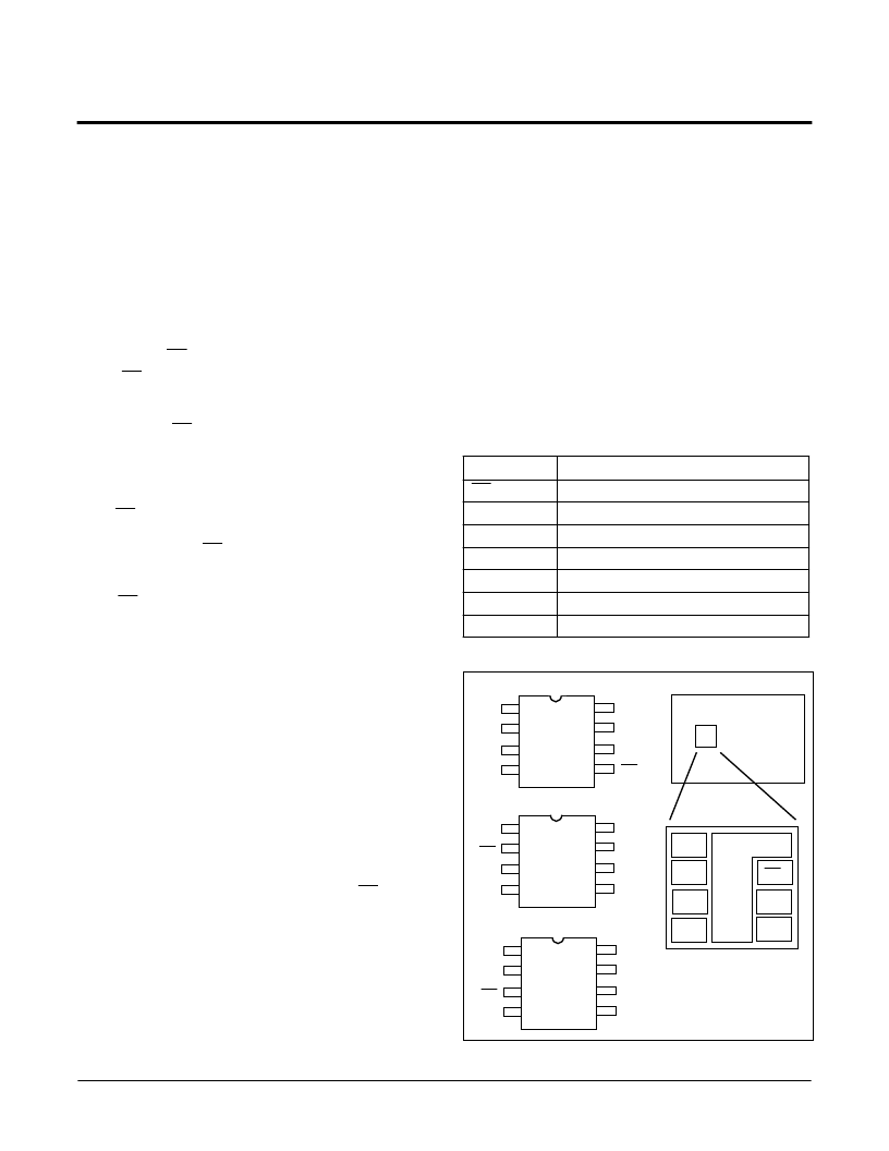
PIN NAMES
PIN CONFIGURATION
Symbol
CS
SDA
SCL
RST
Vcc
Vss
NC
Description
Chip Select Input
Serial Data Input/Output
Serial Clock Input
Reset Input
Supply Voltage
Ground
No Connect
CS
SDA
V
CC
RST
SCL
NC
1
2
3
4
7
8
6
5
SOIC
V
CC
RST
SCL
V
SS
NC
SDA
Smart Card
CS
NC
NC
GND
CS
SDA
VCC
NC
RST
SCL
NC
1
2
3
4
7
8
6
5
MSOP
VSS
NC
RST
SCL
SDA
CS
Vss
1
2
3
4
7
8
6
5
PDIP
V
CC
NC
相關PDF資料 |
PDF描述 |
|---|---|
| X76F101Y-3.0 | EEPROM |
| X76F101YI | EEPROM |
| X76F101YI-3.0 | EEPROM |
| X76F102M8-2.0 | Serial EEPROM |
| X76F102M8I-2.0 | Serial EEPROM |
相關代理商/技術(shù)參數(shù) |
參數(shù)描述 |
|---|---|
| X76F101Y-3.0 | 制造商:未知廠家 制造商全稱:未知廠家 功能描述:EEPROM |
| X76F101YG | 制造商:ICMIC 制造商全稱:IC MICROSYSTEMS 功能描述:Secure SerialFlash |
| X76F101YG-3.0 | 制造商:ICMIC 制造商全稱:IC MICROSYSTEMS 功能描述:Secure SerialFlash |
| X76F101YI | 制造商:ICMIC 制造商全稱:IC MICROSYSTEMS 功能描述:Secure SerialFlash |
| X76F101YI-3.0 | 制造商:未知廠家 制造商全稱:未知廠家 功能描述:EEPROM |
發(fā)布緊急采購,3分鐘左右您將得到回復。