- 您現(xiàn)在的位置:買賣IC網(wǎng) > PDF目錄371296 > X9409 (Intersil Corporation) Low Noise/Low Power/2-Wire Bus PDF資料下載
參數(shù)資料
| 型號: | X9409 |
| 廠商: | Intersil Corporation |
| 英文描述: | Low Noise/Low Power/2-Wire Bus |
| 中文描述: | 低噪音/低Power/2-Wire巴士 |
| 文件頁數(shù): | 2/21頁 |
| 文件大小: | 407K |
| 代理商: | X9409 |

X9409
– Preliminary Information
Characteristics subject to change without notice.
2 of 21
REV 1.6 1/30/03
www.xicor.com
PIN DESCRIPTIONS
Host Interface Pins
Serial Clock (SCL)
The SCL input is used to clock data into and out of the
X9409.
Serial Data (SDA)
SDA is a bidirectional pin used to transfer data into
and out of the device. It is an open drain output and
may be wire-ORed with any number of open drain or
open collector outputs. An open drain output requires
the use of a pull-up resistor. For selecting typical
values, refer to the guidelines for calculating typical
values on the bus pull-up resistors graph.
Device Address (A
The address inputs are used to set the least significant
4 bits of the 8-bit slave address. A match in the slave
address serial data stream must be made with the
address input in order to initiate communication with
the X9409. A maximum of 16 devices may occupy the
2-wire serial bus.
0
–
A
3
)
Potentiometer Pins
V
The V
terminal connections on either end of a mechanical
potentiometer.
H0
/R
H0
–V
/R
H3
and V
/R
H3
, V
/R
L0
/R
inputs are equivalent to the
L0
–V
L3
/R
L3
H
H
L
L
V
The wiper outputs are equivalent to the wiper output of
a mechanical potentiometer.
W0
/R
W0
–V
W3
/R
W3
Hardware Write Protect Input (WP)
The WP pin when low prevents nonvolatile writes to
the Data Registers.
PIN NAMES
Symbol
Description
SCL
SDA
A0-A3
V
H0
V
L0
V
W0
Serial Clock
Serial Data
Device Address
Potentiometer Pin
(terminal equivalent)
Potentiometer Pin
(wiper equivalent)
Hardware Write Protection
System Supply Voltage
System Ground (Digital)
No Connection
/R
/R
H0
L0
–V
–V
H3
L3
–V
/R
/R
H3
L3
/R
,
/R
W0
W3
W3
WP
V
CC
V
SS
NC
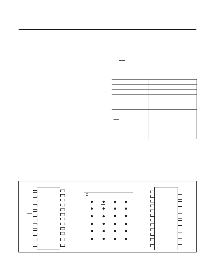
PIN CONFIGURATION
V
CC
V
L0
/R
L0
V
H0
/R
H0
V
W0
/R
W0
WP
SDA
A
1
1
2
3
4
5
6
7
8
9
10
24
23
22
21
20
19
18
17
16
15
NC
V
L3
/R
L3
V
H3
/R
H3
V
W3
/R
W3
A
0
NC
A
3
SCL
V
L2
/R
L2
V
H2
/R
H2
SOIC
X9409
V
SS
14
13
11
12
A
2
V
L1
/R
L1
V
H1
/R
H1
V
W1
/R
W1
V
W2
/R
W2
NC
SDA
A
1
V
H2
/R
H2
V
L2
/R
L2
1
2
3
4
5
6
7
8
9
10
24
23
22
21
20
19
18
17
16
15
WP
A
2
V
W0
/R
W0
V
H0
/R
H0
V
L0
/R
L0
V
CC
NC
V
L3
/R
L3
V
H3
/R
H3
V
W3
/R
W3
TSSOP
X9409
V
W2
/R
W2
14
13
11
12
A
3
V
L1
/R
L1
V
H1
/R
H1
V
W1
/R
W1
A
0
NC
NC
SCL
V
SS
2
3
4
A
B
C
D
E
F
Top View–Bumps Down
V
W0
/R
W0
V
L0
/R
L0
NC
A0
A
3
V
L1
/R
L1
V
CC
V
L3
/R
L3
V
W3
/R
W3
NC
SDA
V
W1
/R
W1
SCL
V
L2
/R
L2
WP
NC
V
H0
/R
H0
V
H1
/R
H1
V
H3
/R
H3
V
H2
/R
H2
V
SS
V
W2
/R
W2
A
2
A
1
1
CSP
相關(guān)PDF資料 |
PDF描述 |
|---|---|
| X9409WS24 | Low Noise/Low Power/2-Wire Bus |
| X9409WS24-2.7 | Low Noise/Low Power/2-Wire Bus |
| X9409WS24I | Low Noise/Low Power/2-Wire Bus |
| X9409WS24I-2.7 | Low Noise/Low Power/2-Wire Bus |
| X9409WS24IZ | Low Noise/Low Power/2-Wire Bus |
相關(guān)代理商/技術(shù)參數(shù) |
參數(shù)描述 |
|---|---|
| X9409_06 | 制造商:INTERSIL 制造商全稱:Intersil Corporation 功能描述:Quad Digitally Controlled Potentiometers |
| X9409WB241 | 制造商:XICOR 制造商全稱:Xicor Inc. 功能描述:Quad Digitally Controlled Potentiometers |
| X9409WB241-2.7 | 制造商:XICOR 制造商全稱:Xicor Inc. 功能描述:Quad Digitally Controlled Potentiometers |
| X9409WB241I | 制造商:XICOR 制造商全稱:Xicor Inc. 功能描述:Quad Digitally Controlled Potentiometers |
| X9409WB241I-2.7 | 制造商:XICOR 制造商全稱:Xicor Inc. 功能描述:Quad Digitally Controlled Potentiometers |
發(fā)布緊急采購,3分鐘左右您將得到回復(fù)。