- 您現(xiàn)在的位置:買賣IC網(wǎng) > PDF目錄4274 > XC2V40-5CSG144I (Xilinx Inc)IC FPGA VIRTEX-II 40K 144-CSBGA PDF資料下載
參數(shù)資料
| 型號: | XC2V40-5CSG144I |
| 廠商: | Xilinx Inc |
| 文件頁數(shù): | 223/318頁 |
| 文件大?。?/td> | 0K |
| 描述: | IC FPGA VIRTEX-II 40K 144-CSBGA |
| 產(chǎn)品變化通告: | FPGA Family Discontinuation 18/Apr/2011 |
| 標(biāo)準(zhǔn)包裝: | 198 |
| 系列: | Virtex®-II |
| LAB/CLB數(shù): | 64 |
| RAM 位總計(jì): | 73728 |
| 輸入/輸出數(shù): | 88 |
| 門數(shù): | 40000 |
| 電源電壓: | 1.425 V ~ 1.575 V |
| 安裝類型: | 表面貼裝 |
| 工作溫度: | -40°C ~ 100°C |
| 封裝/外殼: | 144-TFBGA,CSPBGA |
| 供應(yīng)商設(shè)備封裝: | 144-LCSBGA(12x12) |
第1頁第2頁第3頁第4頁第5頁第6頁第7頁第8頁第9頁第10頁第11頁第12頁第13頁第14頁第15頁第16頁第17頁第18頁第19頁第20頁第21頁第22頁第23頁第24頁第25頁第26頁第27頁第28頁第29頁第30頁第31頁第32頁第33頁第34頁第35頁第36頁第37頁第38頁第39頁第40頁第41頁第42頁第43頁第44頁第45頁第46頁第47頁第48頁第49頁第50頁第51頁第52頁第53頁第54頁第55頁第56頁第57頁第58頁第59頁第60頁第61頁第62頁第63頁第64頁第65頁第66頁第67頁第68頁第69頁第70頁第71頁第72頁第73頁第74頁第75頁第76頁第77頁第78頁第79頁第80頁第81頁第82頁第83頁第84頁第85頁第86頁第87頁第88頁第89頁第90頁第91頁第92頁第93頁第94頁第95頁第96頁第97頁第98頁第99頁第100頁第101頁第102頁第103頁第104頁第105頁第106頁第107頁第108頁第109頁第110頁第111頁第112頁第113頁第114頁第115頁第116頁第117頁第118頁第119頁第120頁第121頁第122頁第123頁第124頁第125頁第126頁第127頁第128頁第129頁第130頁第131頁第132頁第133頁第134頁第135頁第136頁第137頁第138頁第139頁第140頁第141頁第142頁第143頁第144頁第145頁第146頁第147頁第148頁第149頁第150頁第151頁第152頁第153頁第154頁第155頁第156頁第157頁第158頁第159頁第160頁第161頁第162頁第163頁第164頁第165頁第166頁第167頁第168頁第169頁第170頁第171頁第172頁第173頁第174頁第175頁第176頁第177頁第178頁第179頁第180頁第181頁第182頁第183頁第184頁第185頁第186頁第187頁第188頁第189頁第190頁第191頁第192頁第193頁第194頁第195頁第196頁第197頁第198頁第199頁第200頁第201頁第202頁第203頁第204頁第205頁第206頁第207頁第208頁第209頁第210頁第211頁第212頁第213頁第214頁第215頁第216頁第217頁第218頁第219頁第220頁第221頁第222頁當(dāng)前第223頁第224頁第225頁第226頁第227頁第228頁第229頁第230頁第231頁第232頁第233頁第234頁第235頁第236頁第237頁第238頁第239頁第240頁第241頁第242頁第243頁第244頁第245頁第246頁第247頁第248頁第249頁第250頁第251頁第252頁第253頁第254頁第255頁第256頁第257頁第258頁第259頁第260頁第261頁第262頁第263頁第264頁第265頁第266頁第267頁第268頁第269頁第270頁第271頁第272頁第273頁第274頁第275頁第276頁第277頁第278頁第279頁第280頁第281頁第282頁第283頁第284頁第285頁第286頁第287頁第288頁第289頁第290頁第291頁第292頁第293頁第294頁第295頁第296頁第297頁第298頁第299頁第300頁第301頁第302頁第303頁第304頁第305頁第306頁第307頁第308頁第309頁第310頁第311頁第312頁第313頁第314頁第315頁第316頁第317頁第318頁
Virtex-II Platform FPGAs: Introduction and Overview
R
DS031-1 (v3.5) November 5, 2007
Module 1 of 4
Product Specification
2
General Description
The Virtex-II family is a platform FPGA developed for high
performance from low-density to high-density designs that
are based on IP cores and customized modules. The family
delivers complete solutions for telecommunication, wire-
less, networking, video, and DSP applications, including
PCI, LVDS, and DDR interfaces.
The leading-edge 0.15 m / 0.12 m CMOS 8-layer metal
process and the Virtex-II architecture are optimized for high
speed with low power consumption. Combining a wide vari-
ety of flexible features and a large range of densities up to
10 million system gates, the Virtex-II family enhances pro-
grammable logic design capabilities and is a powerful alter-
native to mask-programmed gates arrays. As shown in
Table 1, the Virtex-II family comprises 11 members, ranging
from 40K to 8M system gates.
Packaging
Offerings include ball grid array (BGA) packages with
0.80 mm, 1.00 mm, and 1.27 mm pitches. In addition to tra-
ditional wire-bond interconnects, flip-chip interconnect is
used in some of the BGA offerings. The use of flip-chip
interconnect offers more I/Os than is possible in wire-bond
versions of the similar packages. Flip-chip construction
offers the combination of high pin count with high thermal
capacity.
Wire-bond packages CS, FG, and BG are optionally avail-
abe in Pb-free versions CSG, FGG, and BGG. See Virtex-II
Table 2 shows the maximum number of user I/Os available.
The Virtex-II device/package combination table (Table 6 at
the end of this section) details the maximum number of I/Os
for each device and package using wire-bond or flip-chip
technology.
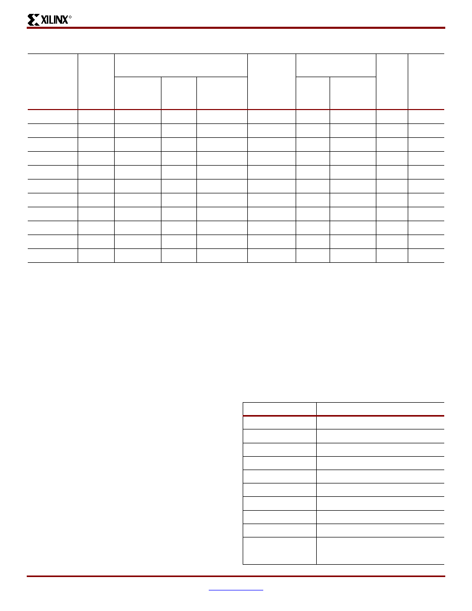
Table 1: Virtex-II Field-Programmable Gate Array Family Members
Device
System
Gates
CLB
(1 CLB = 4 slices = Max 128 bits)
Multiplier
Blocks
SelectRAM Blocks
DCMs
Max I/O
Pads(1)
Array
Row x Col.
Slices
Maximum
Distributed
RAM Kbits
18 Kbit
Blocks
Max RAM
(Kbits)
XC2V40
40K
8 x 8
256
8
4
72
4
88
XC2V80
80K
16 x 8
512
16
8
144
4
120
XC2V250
250K
24 x 16
1,536
48
24
432
8
200
XC2V500
500K
32 x 24
3,072
96
32
576
8
264
XC2V1000
1M
40 x 32
5,120
160
40
720
8
432
XC2V1500
1.5M
48 x 40
7,680
240
48
864
8
528
XC2V2000
2M
56 x 48
10,752
336
56
1,008
8
624
XC2V3000
3M
64 x 56
14,336
448
96
1,728
12
720
XC2V4000
4M
80 x 72
23,040
720
120
2,160
12
912
XC2V6000
6M
96 x 88
33,792
1,056
144
2,592
12
1,104
XC2V8000
8M
112 x 104
46,592
1,456
168
3,024
12
1,108
Notes:
1.
See details in Table 2, “Maximum Number of User I/O Pads”
.
Table 2: Maximum Number of User I/O Pads
Device
Wire-Bond
Flip-Chip
XC2V40
88
-
XC2V80
120
-
XC2V250
200
-
XC2V500
264
-
XC2V1000
328
432
XC2V1500
392
528
XC2V2000
-
624
XC2V3000
516
720
XC2V4000
-
912
XC2V6000
-
1,104
XC2V8000
-
1,108
相關(guān)PDF資料 |
PDF描述 |
|---|---|
| XA6SLX9-3CSG324Q | IC FPGA SPARTAN 6 324CSGBGA |
| XC3S400-4FGG456I | SPARTAN-3A FPGA 400K STD 456FBGA |
| XC3S400-5FGG456C | SPARTAN-3A FPGA 400K 456-FBGA |
| XC3S1000-4FT256I | IC FPGA SPARTAN 3 256FTBGA |
| XC3S1000-5FTG256C | SPARTAN-3A FPGA 1M 256-FTBGA |
相關(guān)代理商/技術(shù)參數(shù) |
參數(shù)描述 |
|---|---|
| XC2V40-5FF1152C | 制造商:XILINX 制造商全稱:XILINX 功能描述:Virtex-II 1.5V Field-Programmable Gate Arrays |
| XC2V40-5FF1152I | 制造商:XILINX 制造商全稱:XILINX 功能描述:Virtex-II 1.5V Field-Programmable Gate Arrays |
| XC2V40-5FF1517C | 制造商:XILINX 制造商全稱:XILINX 功能描述:Virtex-II 1.5V Field-Programmable Gate Arrays |
| XC2V40-5FF1517I | 制造商:XILINX 制造商全稱:XILINX 功能描述:Virtex-II 1.5V Field-Programmable Gate Arrays |
| XC2V40-5FF896C | 制造商:XILINX 制造商全稱:XILINX 功能描述:Virtex-II 1.5V Field-Programmable Gate Arrays |
發(fā)布緊急采購,3分鐘左右您將得到回復(fù)。