- 您現(xiàn)在的位置:買賣IC網(wǎng) > PDF目錄371339 > XC5206-3PC84I Field Programmable Gate Array (FPGA) PDF資料下載
參數(shù)資料
| 型號: | XC5206-3PC84I |
| 英文描述: | Field Programmable Gate Array (FPGA) |
| 中文描述: | 現(xiàn)場可編程門陣列(FPGA) |
| 文件頁數(shù): | 3/73頁 |
| 文件大小: | 598K |
| 代理商: | XC5206-3PC84I |
第1頁第2頁當(dāng)前第3頁第4頁第5頁第6頁第7頁第8頁第9頁第10頁第11頁第12頁第13頁第14頁第15頁第16頁第17頁第18頁第19頁第20頁第21頁第22頁第23頁第24頁第25頁第26頁第27頁第28頁第29頁第30頁第31頁第32頁第33頁第34頁第35頁第36頁第37頁第38頁第39頁第40頁第41頁第42頁第43頁第44頁第45頁第46頁第47頁第48頁第49頁第50頁第51頁第52頁第53頁第54頁第55頁第56頁第57頁第58頁第59頁第60頁第61頁第62頁第63頁第64頁第65頁第66頁第67頁第68頁第69頁第70頁第71頁第72頁第73頁

R
November 5, 1998 (Version 5.2)
7-85
XC5200 Series Field Programmable Gate Arrays
7
XC3000 family: XC5200 devices support an additional pro-
gramming mode: Peripheral Synchronous.
XC3000 family:The XC5200 family does not support
Power-down, but offers a Global 3-state input that does not
reset any flip-flops.
XC3000 family: The XC5200 family does not provide an
on-chip crystal oscillator amplifier, but it does provide an
internal oscillator from which a variety of frequencies up to
12 MHz are available.
Architectural Overview
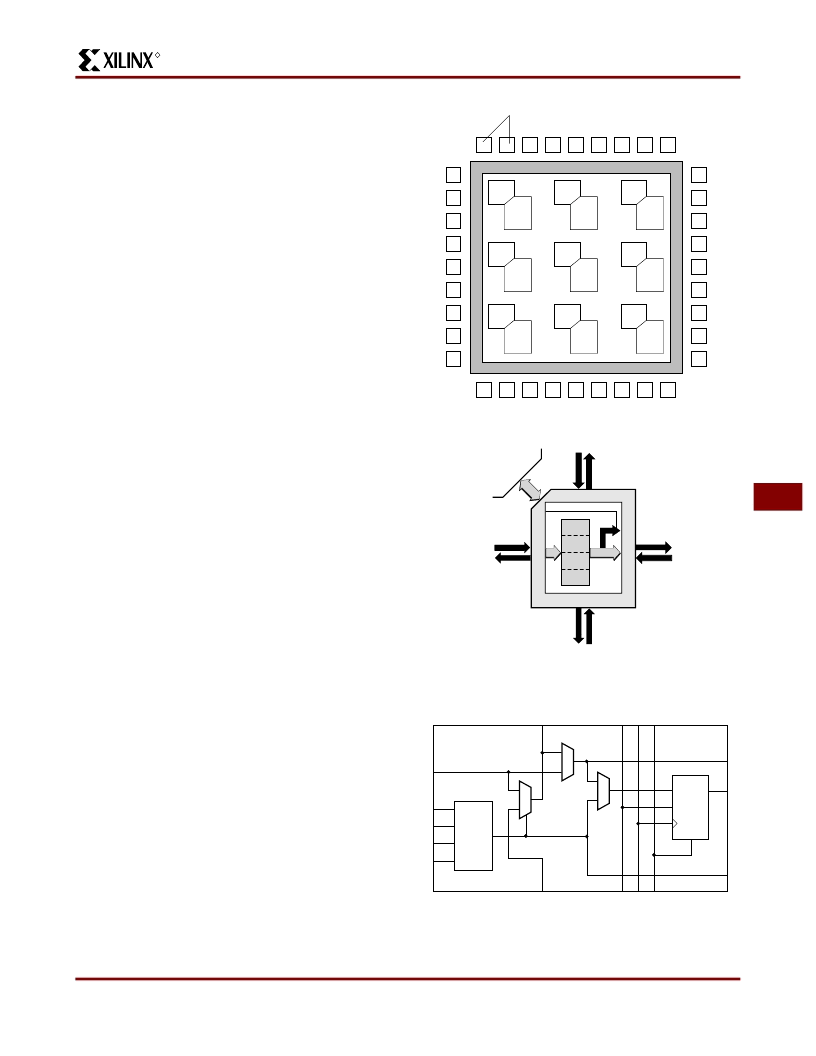
Figure 1
presents a simplified, conceptual overview of the
XC5200 architecture. Similar to conventional FPGAs, the
XC5200 family consists of programmable IOBs, program-
mable logic blocks, and programmable interconnect. Unlike
other FPGAs, however, the logic and local routing
resources of the XC5200 family are combined in flexible
VersaBlocks (
Figure 2
). General-purpose routing connects
to the VersaBlock through the General Routing Matrix
(GRM).
VersaBlock: Abundant Local Routing Plus
Versatile Logic
The basic logic element in each VersaBlock structure is the
Logic Cell, shown in
Figure 3
. Each LC contains a 4-input
function generator (F), a storage device (FD), and control
logic. There are five independent inputs and three outputs
to each LC. The independence of the inputs and outputs
allows the software to maximize the resource utilization
within each LC. Each Logic Cell also contains a direct
feedthrough path that does not sacrifice the use of either
the function generator or the register; this feature is a first
for FPGAs. The storage device is configurable as either a D
flip-flop or a latch. The control logic consists of carry logic
for fast implementation of arithmetic functions, which can
also be configured as a cascade chain allowing decode of
very wide input functions.
Figure 1: XC5200 Architectural Overview
Figure 2: VersaBlock
Figure 3: XC5200 Logic Cell (Four LCs per CLB)
X4955
GRM
Input/Output Blocks (IOBs)
Block
GRM
Block
VersaRing
VersaRing
GRM
Block
GRM
Block
GRM
Block
GRM
Block
GRM
Block
GRM
Block
GRM
Block
V
V
X5707
CLB
LC3
Direct Connects
TS
GRM
LIM
4
4
4
4
4
LC2
LC1
LC0
4
4
4
4
24
X4956
F4
F3
F
FD
F2
F1
D
Q
X
DO
DI
CO
CI
CE CK
CLR
相關(guān)PDF資料 |
PDF描述 |
|---|---|
| XC5206-3PG191I | Field Programmable Gate Array (FPGA) |
| XC5206-3PQ100I | Field Programmable Gate Array (FPGA) |
| XC5206-4PQ100I | Field Programmable Gate Array (FPGA) |
| XC5206-4PQ160I | Field Programmable Gate Array (FPGA) |
| XC5206-4PQ208I | Field Programmable Gate Array (FPGA) |
相關(guān)代理商/技術(shù)參數(shù) |
參數(shù)描述 |
|---|---|
| XC5206-3PG156C | 制造商:XILINX 制造商全稱:XILINX 功能描述:Field Programmable Gate Arrays |
| XC5206-3PG191C | 制造商:XILINX 制造商全稱:XILINX 功能描述:Field Programmable Gate Arrays |
| XC5206-3PG191I | 制造商:未知廠家 制造商全稱:未知廠家 功能描述:Field Programmable Gate Array (FPGA) |
| XC5206-3PG223C | 制造商:XILINX 制造商全稱:XILINX 功能描述:Field Programmable Gate Arrays |
| XC5206-3PG299C | 制造商:XILINX 制造商全稱:XILINX 功能描述:Field Programmable Gate Arrays |
發(fā)布緊急采購,3分鐘左右您將得到回復(fù)。