- 您現(xiàn)在的位置:買賣IC網(wǎng) > PDF目錄4174 > XC5206-5TQ144C (Xilinx Inc)IC FPGA 196 CLB'S 144-TQFP PDF資料下載
參數(shù)資料
| 型號(hào): | XC5206-5TQ144C |
| 廠商: | Xilinx Inc |
| 文件頁(yè)數(shù): | 34/73頁(yè) |
| 文件大小: | 0K |
| 描述: | IC FPGA 196 CLB'S 144-TQFP |
| 產(chǎn)品變化通告: | XC1700 PROMs,XC5200,HQ,SCD Parts Discontinuation 19/Jul/2010 |
| 標(biāo)準(zhǔn)包裝: | 60 |
| 系列: | XC5200 |
| LAB/CLB數(shù): | 196 |
| 邏輯元件/單元數(shù): | 784 |
| 輸入/輸出數(shù): | 117 |
| 門數(shù): | 10000 |
| 電源電壓: | 4.75 V ~ 5.25 V |
| 安裝類型: | 表面貼裝 |
| 工作溫度: | 0°C ~ 85°C |
| 封裝/外殼: | 144-LQFP |
| 供應(yīng)商設(shè)備封裝: | 144-TQFP(20x20) |
| 其它名稱: | 122-1143 |
第1頁(yè)第2頁(yè)第3頁(yè)第4頁(yè)第5頁(yè)第6頁(yè)第7頁(yè)第8頁(yè)第9頁(yè)第10頁(yè)第11頁(yè)第12頁(yè)第13頁(yè)第14頁(yè)第15頁(yè)第16頁(yè)第17頁(yè)第18頁(yè)第19頁(yè)第20頁(yè)第21頁(yè)第22頁(yè)第23頁(yè)第24頁(yè)第25頁(yè)第26頁(yè)第27頁(yè)第28頁(yè)第29頁(yè)第30頁(yè)第31頁(yè)第32頁(yè)第33頁(yè)當(dāng)前第34頁(yè)第35頁(yè)第36頁(yè)第37頁(yè)第38頁(yè)第39頁(yè)第40頁(yè)第41頁(yè)第42頁(yè)第43頁(yè)第44頁(yè)第45頁(yè)第46頁(yè)第47頁(yè)第48頁(yè)第49頁(yè)第50頁(yè)第51頁(yè)第52頁(yè)第53頁(yè)第54頁(yè)第55頁(yè)第56頁(yè)第57頁(yè)第58頁(yè)第59頁(yè)第60頁(yè)第61頁(yè)第62頁(yè)第63頁(yè)第64頁(yè)第65頁(yè)第66頁(yè)第67頁(yè)第68頁(yè)第69頁(yè)第70頁(yè)第71頁(yè)第72頁(yè)第73頁(yè)

R
XC5200 Series Field Programmable Gate Arrays
7-86
November 5, 1998 (Version 5.2)
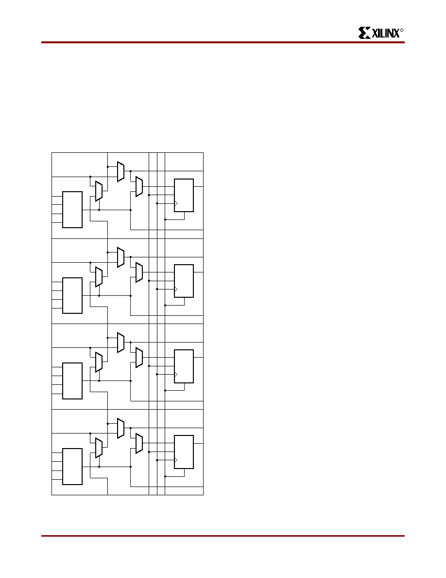
The XC5200 CLB consists of four LCs, as shown in
Figure 4. Each CLB has 20 independent inputs and 12
independent outputs. The top and bottom pairs of LCs can
be configured to implement 5-input functions. The chal-
lenge of FPGA implementation software has always been
to maximize the usage of logic resources. The XC5200
family addresses this issue by surrounding each CLB with
two types of local interconnect — the Local Interconnect
Matrix (LIM) and direct connects. These two interconnect
resources, combined with the CLB, form the VersaBlock,
represented in Figure 2.
The LIM provides 100% connectivity of the inputs and out-
puts of each LC in a given CLB. The benefit of the LIM is
that no general routing resources are required to connect
feedback paths within a CLB. The LIM connects to the
GRM via 24 bidirectional nodes.
The direct connects allow immediate connections to neigh-
boring CLBs, once again without using any of the general
interconnect. These two layers of local routing resource
improve the granularity of the architecture, effectively mak-
ing the XC5200 family a “sea of logic cells.” Each
Versa-Block has four 3-state buffers that share a common
enable line and directly drive horizontal and vertical Lon-
glines, creating robust on-chip bussing capability. The
VersaBlock allows fast, local implementation of logic func-
tions, effectively implementing user designs in a hierarchi-
cal fashion. These resources also minimize local routing
congestion and improve the efficiency of the general inter-
connect, which is used for connecting larger groups of
logic. It is this combination of both fine-grain and
coarse-grain architecture attributes that maximize logic uti-
lization in the XC5200 family. This symmetrical structure
takes full advantage of the third metal layer, freeing the
placement software to pack user logic optimally with mini-
mal routing restrictions.
VersaRing I/O Interface
The interface between the IOBs and core logic has been
redesigned in the XC5200 family. The IOBs are completely
decoupled from the core logic. The XC5200 IOBs contain
dedicated boundary-scan logic for added board-level test-
ability, but do not include input or output registers. This
approach allows a maximum number of IOBs to be placed
around the device, improving the I/O-to-gate ratio and
decreasing the cost per I/O. A “freeway” of interconnect
cells surrounding the device forms the VersaRing, which
provides connections from the IOBs to the internal logic.
These incremental routing resources provide abundant
connections from each IOB to the nearest VersaBlock, in
addition to Longline connections surrounding the device.
The VersaRing eliminates the historic trade-off between
high logic utilization and pin placement flexibility. These
incremental edge resources give users increased flexibility
in preassigning (i.e., locking) I/O pins before completing
their logic designs. This ability accelerates time-to-market,
since PCBs and other system components can be manu-
factured concurrent with the logic design.
General Routing Matrix
The GRM is functionally similar to the switch matrices
found in other architectures, but it is novel in its tight cou-
pling to the logic resources contained in the VersaBlocks.
Advanced simulation tools were used during the develop-
ment of the XC5200 architecture to determine the optimal
level of routing resources required. The XC5200 family
contains six levels of interconnect hierarchy — a series of
Figure 4: Configurable Logic Block
X4957
F4
F3
F
FD
LC3
LC2
LC1
LC0
F2
F1
DQ
X
DO
DI
CO
F4
F3
F
FD
F2
F1
DQ
X
DO
DI
F4
F3
F
FD
F2
F1
DQ
X
DO
DI
F4
F3
F
FD
F2
F1
DQ
X
DO
DI
CI
CE CK
CLR
LC0
Product Obsolete or Under Obsolescence
相關(guān)PDF資料 |
PDF描述 |
|---|---|
| ABB105DHRR | CONN CARD EXTEND 210POS .050" |
| XC5206-5PQ208C | IC FPGA 196 CLB'S 208-PQFP |
| ABB65DHAS | CONN EDGECARD 130PS R/A .050 SLD |
| XC5206-6PQ160C | IC FPGA 196 CLB'S 160-PQFP |
| GSC49DTEI | CONN EDGECARD 98POS .100 EYELET |
相關(guān)代理商/技術(shù)參數(shù) |
參數(shù)描述 |
|---|---|
| XC5206-5TQ144C0262 | 制造商:Xilinx 功能描述: |
| XC5206-5TQ144I | 制造商:未知廠家 制造商全稱:未知廠家 功能描述:Field Programmable Gate Array (FPGA) |
| XC5206-5TQ176C | 制造商:Xilinx 功能描述: 制造商:Xilinx 功能描述:FPGA, 196 CLBS, 6000 GATES, 83 MHz, PQFP176 |
| XC5206-5VQ100C | 制造商:Xilinx 功能描述: |
| XC5206-5VQ100I | 制造商:未知廠家 制造商全稱:未知廠家 功能描述:Field Programmable Gate Array (FPGA) |
發(fā)布緊急采購(gòu),3分鐘左右您將得到回復(fù)。