- 您現(xiàn)在的位置:買賣IC網(wǎng) > PDF目錄225573 > XC7K420T-1FFG1156E (XILINX INC) FPGA, PBGA1156 PDF資料下載
參數(shù)資料
| 型號: | XC7K420T-1FFG1156E |
| 廠商: | XILINX INC |
| 元件分類: | FPGA |
| 英文描述: | FPGA, PBGA1156 |
| 封裝: | LEAD FREE, FBGA-1156 |
| 文件頁數(shù): | 36/50頁 |
| 文件大小: | 1218K |
| 代理商: | XC7K420T-1FFG1156E |
第1頁第2頁第3頁第4頁第5頁第6頁第7頁第8頁第9頁第10頁第11頁第12頁第13頁第14頁第15頁第16頁第17頁第18頁第19頁第20頁第21頁第22頁第23頁第24頁第25頁第26頁第27頁第28頁第29頁第30頁第31頁第32頁第33頁第34頁第35頁當前第36頁第37頁第38頁第39頁第40頁第41頁第42頁第43頁第44頁第45頁第46頁第47頁第48頁第49頁第50頁
Kintex-7 FPGAs Data Sheet: DC and Switching Characteristics
DS182 (v1.1) April 1, 2011
Advance Product Specification
41
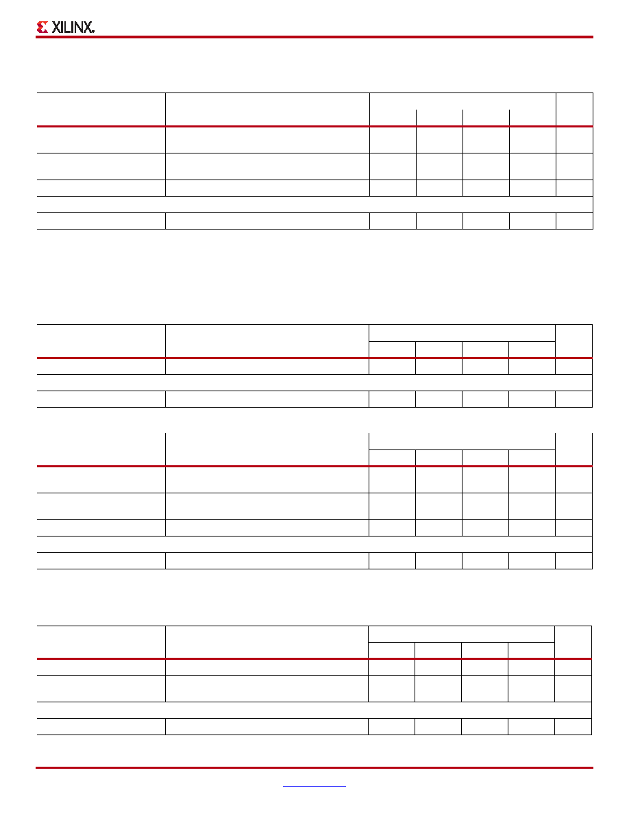
Clock Buffers and Networks
Table 41: Global Clock Switching Characteristics (Including BUFGCTRL)
Symbol
Description
Speed Grade
Units
-3
-2
-1
-1L
CE pins Setup/Hold
0.10/
0.04
0.12/
0.05
0.15/
0.05
ns
S pins Setup/Hold
0.10/
0.04
0.12/
0.05
0.15/
0.05
ns
TBCCKO_O(2)
BUFGCTRL delay from I0/I1 to O
0.08
0.09
0.11
ns
Maximum Frequency
FMAX_BUFG
Global clock tree (BUFG)
710
625
MHz
Notes:
1.
TBCCCK_CE and TBCCKC_CE must be satisfied to assure glitch-free operation of the global clock when switching between clocks. These
parameters do not apply to the BUFGMUX primitive that assures glitch-free operation. The other global clock setup and hold times are
optional; only needing to be satisfied if device operation requires simulation matches on a cycle-for-cycle basis when switching between
clocks.
2.
TBGCKO_O (BUFG delay from I0 to O) values are the same as TBCCKO_O values.
Table 42: Input/Output Clock Switching Characteristics (BUFIO)
Symbol
Description
Speed Grade
Units
-3
-2
-1
-1L
TBIOCKO_O
Clock to out delay from I to O
1.14
1.29
1.52
ns
Maximum Frequency
FMAX_BUFIO
I/O clock tree (BUFIO)
800
650
MHz
Table 43: Regional Clock Buffer Switching Characteristics (BUFR)
Symbol
Description
Speed Grade
Units
-3
-2
-1
-1L
TBRCKO_O
Clock to out delay from
I to O
0.77
0.87
1.03
ns
TBRCKO_O_BYP
Clock to out delay from I to O with Divide Bypass
attribute set
0.39
0.44
0.53
ns
TBRDO_O
Propagation delay from CLR to O
0.67
0.76
0.89
ns
Maximum Frequency
FMAX_BUFR(1)
Regional clock tree (BUFR)
575
484
345
MHz
Notes:
1.
The maximum input frequency to the BUFR is the BUFIO FMAX frequency.
Table 44: Horizontal Clock Buffer Switching Characteristics (BUFH)
Symbol
Description
Speed Grade
Units
-3
-2
-1
-1L
TBHCKO_O
BUFH delay from I to O
0.07
0.09
0.11
ns
TBHCCK_CE/TBHCKC_CE
CE pin Setup and Hold
0.09/
0.05
0.11/
0.05
0.14/
0.06
ns
Maximum Frequency
FMAX_BUFH
Horizontal clock buffer (BUFH)
710
625
MHz
相關(guān)PDF資料 |
PDF描述 |
|---|---|
| XC7K420T-1FFG1156I | FPGA, PBGA1156 |
| XC7K420T-1FFG901C | FPGA, PBGA900 |
| XC7K420T-1FFG901E | FPGA, PBGA900 |
| XC7K420T-1FFG901I | FPGA, PBGA900 |
| XC7K420T-1LFFG1156C | FPGA, PBGA1156 |
相關(guān)代理商/技術(shù)參數(shù) |
參數(shù)描述 |
|---|---|
| XC7K420T-1FFG1156I | 制造商:Xilinx 功能描述:KINTEX-7 - Trays 制造商:Xilinx 功能描述:IC FPGA 420K KINTEX-7 1156FBGA |
| XC7K420T-1FFG901C | 制造商:Xilinx 功能描述:KINTEX-7 - Trays 制造商:Xilinx 功能描述:IC FPGA 420K KINTEX-7 901FBGA |
| XC7K420T-1FFG901I | 制造商:Xilinx 功能描述:KINTEX-7 - Trays 制造商:Xilinx 功能描述:IC FPGA 380 I/O 901FCBGA 制造商:Xilinx 功能描述:IC FPGA 420K KINTEX-7 901FBGA |
| XC7K420T-2FF1156C | 制造商:Xilinx 功能描述:KINTEX-7 - Trays 制造商:Xilinx 功能描述:IC FPGA 400 I/O 1156FCBGA |
| XC7K420T-2FF1156I | 制造商:Xilinx 功能描述:KINTEX-7 - Trays 制造商:Xilinx 功能描述:IC FPGA 400 I/O 1156FCBGA |
發(fā)布緊急采購,3分鐘左右您將得到回復(fù)。