- 您現(xiàn)在的位置:買賣IC網(wǎng) > PDF目錄225573 > XC7K420T-1FFG1156I (XILINX INC) FPGA, PBGA1156 PDF資料下載
參數(shù)資料
| 型號: | XC7K420T-1FFG1156I |
| 廠商: | XILINX INC |
| 元件分類: | FPGA |
| 英文描述: | FPGA, PBGA1156 |
| 封裝: | LEAD FREE, FBGA-1156 |
| 文件頁數(shù): | 28/50頁 |
| 文件大小: | 1218K |
| 代理商: | XC7K420T-1FFG1156I |
第1頁第2頁第3頁第4頁第5頁第6頁第7頁第8頁第9頁第10頁第11頁第12頁第13頁第14頁第15頁第16頁第17頁第18頁第19頁第20頁第21頁第22頁第23頁第24頁第25頁第26頁第27頁當前第28頁第29頁第30頁第31頁第32頁第33頁第34頁第35頁第36頁第37頁第38頁第39頁第40頁第41頁第42頁第43頁第44頁第45頁第46頁第47頁第48頁第49頁第50頁
Kintex-7 FPGAs Data Sheet: DC and Switching Characteristics
DS182 (v1.1) April 1, 2011
Advance Product Specification
34
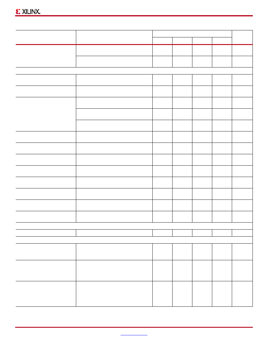
TRCKO_RDADDR_ECC and
TRCKO_RDADDR_ECC_REG
Clock CLK to RDADDR output with ECC
(without output register)
0.64
0.70
0.80
ns, Max
Clock CLK to RDADDR output with ECC
(with output register)
0.69
0.77
0.88
ns, Max
Setup and Hold Times Before/After Clock CLK
TRCCK_ADDRA/TRCKC_ADDRA
ADDR inputs(8)
0.37/
0.21
0.40/
0.23
0.45/
0.25
ns, Min
TRDCK_DI/TRCKD_DI
DIN inputs(9)
0.87/
0.22
0.99/
0.23
1.18/
0.24
ns, Min
TRDCK_DI_ECC/TRCKD_DI_ECC
DIN inputs with block RAM ECC in
standard mode(9)
0.35/
0.22
0.41/
0.23
0.52/
0.24
ns, Min
DIN inputs with block RAM ECC encode
0.76/
0.22
0.88/
0.23
1.05/
0.24
ns, Min
DIN inputs with FIFO ECC in standard
mode(9)
0.87/
0.22
0.99/
0.23
1.18/
0.24
ns, Min
TRCCK_CLK/TRCKC_CLK
Inject single/double bit error in ECC mode
0.51/
0.17
0.58/
0.18
0.68/
0.18
ns, Min
TRCCK_RDEN/TRCKC_RDEN
Block RAM Enable (EN) input
0.36/
0.18
0.39/
0.19
0.44/
0.21
ns, Min
TRCCK_REGCE/TRCKC_REGCE
CE input of output register
0.32/
0.05
0.34/
0.06
0.39/
0.06
ns, Min
TRCCK_RSTREG/TRCKC_RSTREG
Synchronous RSTREG input(10)
0.37/
0.04
0.40/
0.04
0.45/
0.04
ns, Min
TRCCK_RSTRAM/TRCKC_RSTRAM
Synchronous RSTRAM input
0.24/
0.14
0.25/
0.15
0.27/
0.16
ns, Min
TRCCK_WEA/TRCKC_WEA
Write Enable (WE) input (Block RAM only)
0.39/
0.15
0.43/
0.16
0.49/
0.17
ns, Min
TRCCK_WREN/TRCKC_WREN
WREN FIFO inputs
0.46/
0.18
0.51/
0.19
0.59/
0.21
ns, Min
TRCCK_RDEN/TRCKC_RDEN
RDEN FIFO inputs
0.42/
0.18
0.49/
0.19
0.59/
0.21
ns, Min
Reset Delays (Flags)
TRCO_RST
Reset RST to FIFO Flags/Pointers(11)
0.76
0.83
0.94
ns, Max
Maximum Frequency
FMAX_BRAM_WF_NC
Block RAM
(Write first and No change modes)
When not in SDP RF mode
601
544
458
MHz
FMAX_BRAM_RF_PERFORMANCE
Block RAM
(Read first, Performance mode)
When in SDP RF mode but no address
overlap between port A and port B
601
544
458
MHz
FMAX_BRAM_RF_DELAYED_WRITE
Block RAM
(Read first, Delayed_write mode)
When in SDP RF mode and there is
possibility of overlap between port A and
port B addresses
541
485
401
MHz
Table 38: Block RAM and FIFO Switching Characteristics (Cont’d)
Symbol
Description
Speed Grade
Units
-3
-2
-1
-1L
相關(guān)PDF資料 |
PDF描述 |
|---|---|
| XC7K420T-1FFG901C | FPGA, PBGA900 |
| XC7K420T-1FFG901E | FPGA, PBGA900 |
| XC7K420T-1FFG901I | FPGA, PBGA900 |
| XC7K420T-1LFFG1156C | FPGA, PBGA1156 |
| XC7K420T-1LFFG1156E | FPGA, PBGA1156 |
相關(guān)代理商/技術(shù)參數(shù) |
參數(shù)描述 |
|---|---|
| XC7K420T-1FFG901C | 制造商:Xilinx 功能描述:KINTEX-7 - Trays 制造商:Xilinx 功能描述:IC FPGA 420K KINTEX-7 901FBGA |
| XC7K420T-1FFG901I | 制造商:Xilinx 功能描述:KINTEX-7 - Trays 制造商:Xilinx 功能描述:IC FPGA 380 I/O 901FCBGA 制造商:Xilinx 功能描述:IC FPGA 420K KINTEX-7 901FBGA |
| XC7K420T-2FF1156C | 制造商:Xilinx 功能描述:KINTEX-7 - Trays 制造商:Xilinx 功能描述:IC FPGA 400 I/O 1156FCBGA |
| XC7K420T-2FF1156I | 制造商:Xilinx 功能描述:KINTEX-7 - Trays 制造商:Xilinx 功能描述:IC FPGA 400 I/O 1156FCBGA |
| XC7K420T-2FF901C | 制造商:Xilinx 功能描述:KINTEX-7 - Trays 制造商:Xilinx 功能描述:IC FPGA 420K KINTEX-7 901FBGA |
發(fā)布緊急采購,3分鐘左右您將得到回復。