- 您現(xiàn)在的位置:買賣IC網(wǎng) > PDF目錄225573 > XC7K420T-3FFG1156C (XILINX INC) FPGA, PBGA1156 PDF資料下載
參數(shù)資料
| 型號: | XC7K420T-3FFG1156C |
| 廠商: | XILINX INC |
| 元件分類: | FPGA |
| 英文描述: | FPGA, PBGA1156 |
| 封裝: | LEAD FREE, FBGA-1156 |
| 文件頁數(shù): | 42/50頁 |
| 文件大小: | 1218K |
| 代理商: | XC7K420T-3FFG1156C |
第1頁第2頁第3頁第4頁第5頁第6頁第7頁第8頁第9頁第10頁第11頁第12頁第13頁第14頁第15頁第16頁第17頁第18頁第19頁第20頁第21頁第22頁第23頁第24頁第25頁第26頁第27頁第28頁第29頁第30頁第31頁第32頁第33頁第34頁第35頁第36頁第37頁第38頁第39頁第40頁第41頁當(dāng)前第42頁第43頁第44頁第45頁第46頁第47頁第48頁第49頁第50頁
Kintex-7 FPGAs Data Sheet: DC and Switching Characteristics
DS182 (v1.1) April 1, 2011
Advance Product Specification
47
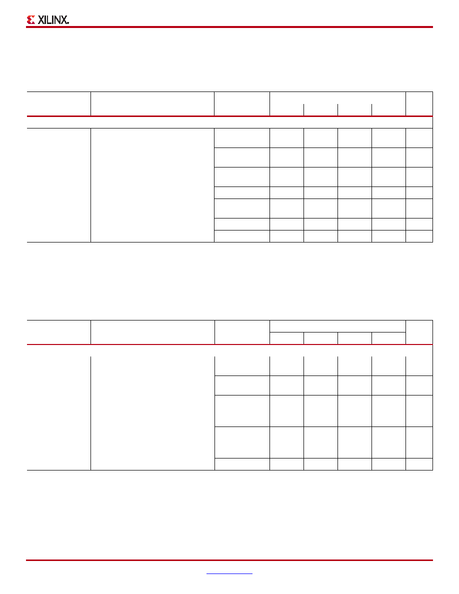
Kintex-7 Device Pin-to-Pin Input Parameter Guidelines
All devices are 100% functionally tested. The representative values for typical pin locations and normal clock loading are
listed in Table 51. Values are expressed in nanoseconds unless otherwise noted.
Table 51: Global Clock Input Setup and Hold Without MMCM/PLL with ZHOLD_DELAY on HR I/O Banks
Symbol
Description
Device
Speed Grade
Units
-3
-2
-1
-1L
Input Setup and Hold Time Relative to Global Clock Input Signal for LVCMOS Standard.(1)
TPSFD/ TPHFD
Full Delay (Legacy Delay or Default
Delay)
Global Clock Input and IFF(2) without
MMCM/PLL with ZHOLD_DELAY on
HR I/O Banks
XC7K70T
–0.41/
2.29
–0.41/
2.57
–0.41/
3.01
ns
XC7K160T
–0.23/
2.11
–0.23/
2.37
–0.23/
2.78
ns
XC7K325T
–0.49/
2.70
–0.49/
3.02
–0.49/
3.53
ns
XC7K355T
ns
XC7K410T
–0.58/
2.83
–0.58/
3.17
–0.58/
3.69
ns
XC7K420T
ns
XC7K480T
ns
Notes:
1.
Setup and Hold times are measured over worst case conditions (process, voltage, temperature). Setup time is measured relative to the
Global Clock input signal using the slowest process, highest temperature, and lowest voltage. Hold time is measured relative to the Global
Clock input signal using the fastest process, lowest temperature, and highest voltage.
2.
IFF = Input Flip-Flop or Latch
3.
A Zero "0" Hold Time listing indicates no hold time or a negative hold time. Negative values can not be guaranteed "best-case", but if a "0"
is listed, there is no positive hold time.
Table 52: Clock-Capable Clock Input Setup and Hold With MMCM
Symbol
Description
Device
Speed Grade
Units
-3
-2
-1
-1L
Input Setup and Hold Time Relative to Global Clock Input Signal for LVCMOS Standard.(1)
TPSMMCMCC/
TPHMMCMCC
No Delay clock-capable clock input and
IFF(2) with MMCM
XC7K70T
1.75/
–0.50
1.94/
–0.50
2.22/
–0.50
ns
XC7K160T
1.80/
–0.49
1.99/
–0.49
2.27/
–0.49
ns
XC7K325T
1.89/
–0.53
2.11/
–0.53
2.43/
–0.53
ns
XC7K355T
ns
XC7K410T
1.89/
–0.53
2.11/
–0.53
2.43/
–0.53
ns
XC7K420T
ns
XC7K480T
ns
Notes:
1.
Setup and Hold times are measured over worst case conditions (process, voltage, temperature). Setup time is measured relative to the
Global Clock input signal using the slowest process, highest temperature, and lowest voltage. Hold time is measured relative to the Global
Clock input signal using the fastest process, lowest temperature, and highest voltage.
2.
IFF = Input Flip-Flop or Latch
3.
Use IBIS to determine any duty-cycle distortion incurred using various standards.
相關(guān)PDF資料 |
PDF描述 |
|---|---|
| XC7K420T-3FFG1156E | FPGA, PBGA1156 |
| XC7K420T-3FFG1156I | FPGA, PBGA1156 |
| XC7K420T-3FFG901C | FPGA, PBGA900 |
| XC7K420T-3FFG901E | FPGA, PBGA900 |
| XC7K420T-3FFG901I | FPGA, PBGA900 |
相關(guān)代理商/技術(shù)參數(shù) |
參數(shù)描述 |
|---|---|
| XC7K420T-3FFG1156E | 制造商:Xilinx 功能描述:KINTEX-7 - Trays 制造商:Xilinx 功能描述:IC FPGA 420K KINTEX-7 1156FBGA |
| XC7K420T-3FFG901E | 制造商:Xilinx 功能描述:KINTEX-7 - Trays 制造商:Xilinx 功能描述:IC FPGA 420K KINTEX-7 901FBGA 制造商:Xilinx 功能描述:IC FPGA 380 I/O 901FCBGA |
| XC7K420T-L2FF1156E | 制造商:Xilinx 功能描述:KINTEX-7 - Trays 制造商:Xilinx 功能描述:IC FPGA 400 I/O 1156FCBGA |
| XC7K420T-L2FF901E | 制造商:Xilinx 功能描述:KINTEX-7 - Trays 制造商:Xilinx 功能描述:IC FPGA 420K KINTEX-7 901FBGA 制造商:Xilinx 功能描述:IC FPGA 380 I/O 901FCBGA |
| XC7K420T-L2FFG1156E | 制造商:Xilinx 功能描述:KINTEX-7 - Trays 制造商:Xilinx 功能描述:IC FPGA 400 I/O 1156FCBGA |
發(fā)布緊急采購,3分鐘左右您將得到回復(fù)。